Lately, much of the talk in the simulation world seems to be about power. Even SI experts are starting to see how power has a material impact on their highspeed data transfer success. With power on the forefront, what effect will that have on the additional design demands of low-frequency supplies? Why should you consider power throughout your design process?
Powering Data Transfer
Signal Integrity at its basic core, studies and describes the effects physical structures can have on a signal as it is transmitted from a source (transmitter) to a destination (receiver), but makes no mention of where the energy for the signal originates, or where it goes once received. Although a bit of oversimplification, the transmitting IC pulls energy from its power supply, bundles it as a bitstream and transmits data to a receiving IC where the energy is dumped onto the ground and eventually returns to the power supply, ready to repeat. Admittedly, today’s high-speed signals are largely differential and draw from multiple power rails, so we aren’t describing the exact current flow. What we are describing is the notion that reliable data transmission involves both a clean path from driver to receiver in addition to a well-designed plan to deliver and return needed power.
In our previous article related to power distribution we discussed capacity. Specifically, we focused on the increasing current demands associated with most new designs and showed the need to ensure our conductors (pins, planes, vias, and etch) were up to the challenge. Today we add another requirement, Responsiveness. Even an IC with ample current supply can experience “power shortage” if the energy needed to transmit the data bitstream isn’t available in time.
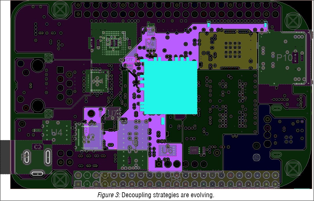
Decoupling Capacitors to the Rescue
Fortunately, this problem has been solved with capacitors. Capacitors provide the board designer the ability to distribute “quick response, power reserves” at selected locations around the board. While the power supply is still responsible for the energy needed to transmit the bitstream, the capacitors provide localized supplemental boosts where needed, subsequently refilling (charging) from the supply. The result is a power distribution network (PDN) capable of supplying each device sufficient current and ensuring delivery is timely enough to support the instantaneous needs of each IC.
Meeting these power boost requirements across the entire design gets increasingly complex with multiple power requirements at differing voltages becoming the norm due to the unique requirements of chips within the design. Determining the quantity, size, and location of these power substations (decoupling capacitors) is not that different than the task faced by a city planner. For example, a well-placed sub-station has little value if it doesn’t directly connect to the population it serves, be it a municipal service or PCB power. For PCB and packaging purposes, ICs access their power source through the very structures we deal in everyday; connectors, vias, etch, and planes. In fact, when we began our series, we explored the use of simple modeling to reliably evaluate a power system’s capacity. Resistors (really resistance) representing the power loss devices experience as they are further from the supply would enable us to generate graphical depictions of the electrical behavior. Frequently, the necessary corrective action could be readily deduced from the graphical depiction alone. With capacity concerns in check, the focus shifts to responsiveness. Can the needed charge be delivered on time?
Deducting Inductance
To answer that, we must add a means to evaluate the power system’s responsiveness. When addressing the instantaneous needs of high-speed ICs, capacitors provide surplus charge, with a level of portability. This enables these reserves to be in closer proximity to the devices who draw from them as the location and means of attachment control their effectiveness. Adding decoupling capacitors of any size, to any location, will yield little benefit if the conduction in the path is insufficient to deliver the charge the capacitors hold to the pins of the chip in need. Therefore, it only makes sense to address the connectivity of each intended capacitor footprint and ensure the best device is selected for each location.
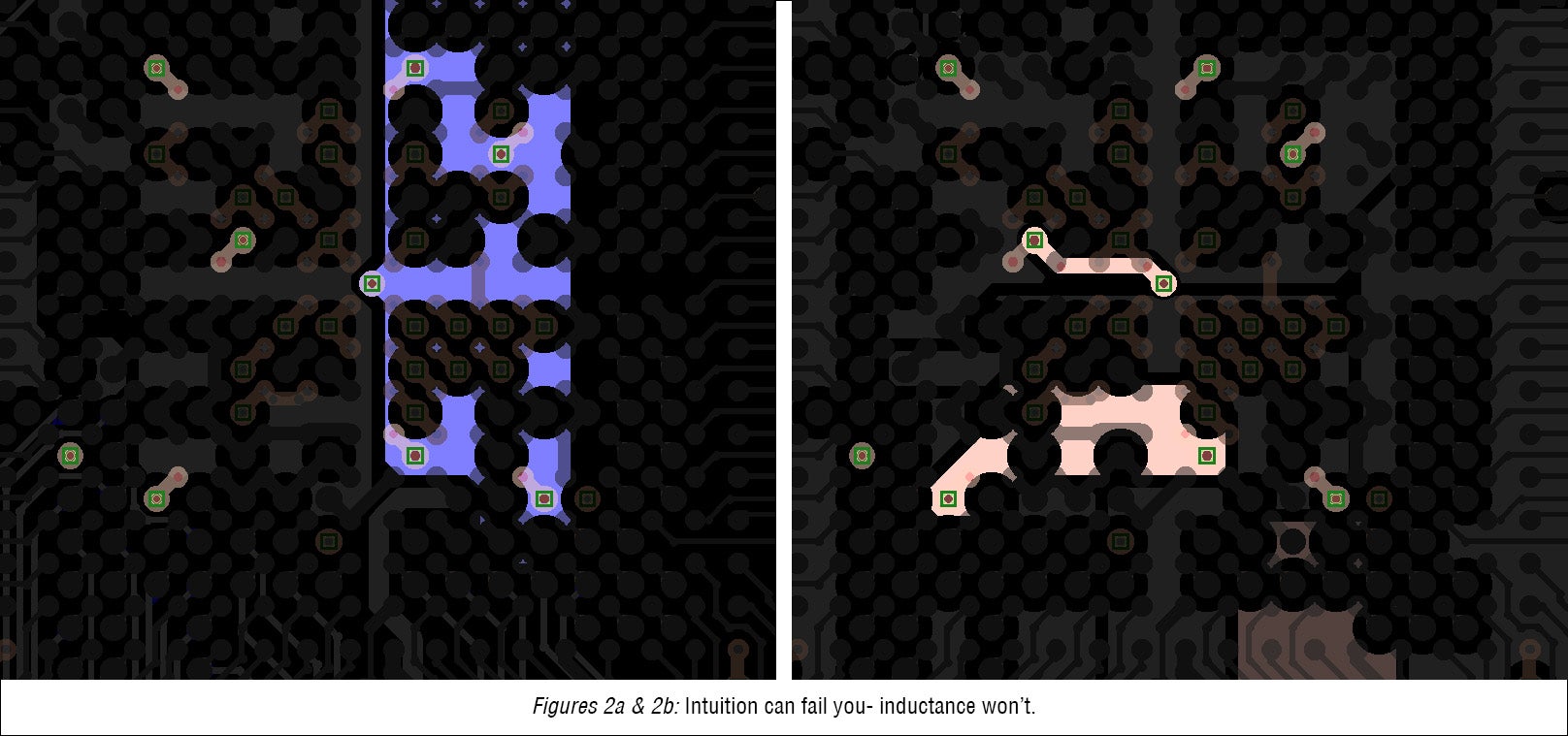
We used resistive loss in our power path to evaluate our DC performance and ensure our PDN would achieve needed DC capacity. In a similar way, we can look to inductance to evaluate our PDN’s responsiveness. In its very definition, inductance is described as “an opposition to a change in current flow,” the identical opposition to change in current that would restrict a PDN’s responsiveness. In short, where responsiveness is a concern, inductance is directly indicative of “good” vs “bad” PDN routing. Fortunately, via the wonders of physics, inductance is quite predictable when we know the materials and the geometry of our conductors, the items we deal with daily in both packaging and PCB domains. Similar to our DC experience, resistive losses accumulate as the distance from the source increases, the inductance also accumulates over length to degrade responsiveness. Not surprisingly, things we do to improve capacity (reduction of cumulative resistance) generally also improve responsiveness (reduction of cumulative inductance).
With Inductance – When things Go Wrong, They Go Wrong Fast
There is, however, a noteworthy difference in the extent to which these factors influence a product’s performance. The resistive losses we associate with a PDN’s capacity, do degrade the output. This compromise is generally observed gradually over large distance and is regulated by the cumulative current demands of all chips sharing power. By contrast, inductive loss, which can quickly defeat a power source’s responsiveness, can be observed at surprisingly small distances. These losses, influenced much more by frequency, as opposed to current, represent an increasingly challenging dilemma every time the data rate ticks up. As board designers now routinely see Interfaces with transfer rates well into the Gigahertz, and even 50 Gig in a few, the demands on the PDN aren’t likely to lessen. Meeting those demands, as we’ll explore in our next article, is readily achievable. However, it does require a multi-level approach. Today’s Power Delivery Networks depend on contribution, not just from the source, but include Regulators, DC-to-DC converters, large “bulk” capacitors, and the familiar 0402 and 0603 ceramics which decorate every PCB we produce. These work horses generally outnumber the others by orders of magnitude and connecting them typically accounts for a significant portion of the power/ground routing. Capacitance from the laminate layers of the PCB, “in-package” and “on-die” capacitance, all become part of the system PDN equation as well. With schematic and stack-up typically fixed, the thing in our control at the time of layout is inductance. We’ve long been accustomed to impedance-controlled etch and understand its relationship to the geometric construction (i.e., thickness and width). In fact, there are tools from several vendors which can accurately predict trace geometry that would result in impedances outside specified requirements. Controlled inductance isn’t as familiar, but there are options that can predict pin-to-pin inductance. Perhaps the most controllable aspect of PDN design, outside of part selection, would be the inductance from power pin to neighboring capacitor and the inductance from supply to the power pins.
Ultimately the most significant “influencer” in terms of supply responsiveness, is the way we connect supply to power pin and capacitor to power pin. Different than most simulation objectives, tools are used to provide guidance in suspected problem areas. These simulators make quick work of decerning the good connections from the bad and can be used to optimize capacitor device selection, effectively fine-tuning even the most complex systems.
Becoming an Inductance Sleuth
While inductance is predictable, it’s not intuitive and the challenge is in identifying inductance issues. For example, planes can often become so perforated with vias, etc. their performance is diminished. Even adding vias to an array used to facilitate high current layer changes can reduce capacity if the drills obstruct the inner vias. While each of these complexities make sense, it is only intuitive once our attention is focused on the problematic area.
Without responsive power availability, designs will fail and will often fail inconsistently making them very hard to debug in the lab. Fortunately, with a proper understanding of PDN responsiveness and inductance design teams can account for these issues upfront to build the effective and responsive PDNs modern devices demand.
Continue reading this series to learn more about incorporating power delivery network analysis into your design process with Jernberg PI #4: Meeting On-time Power Requirements All the Time.
Contact us for more information on how Sigrity can be used to analyze signal integrity and power integrity for PCB Designers.