As the simulation and analysis industry continues to mature, it is evolving from a “mechanism for finding problems” to a “methodology for preventing them”. Many design teams have advanced beyond just checking for violations and are using the tools to make informed design decisions early in a product’s development. This results in better products reaching production floors despite condensed schedules.
A Little History – Chasing Correlation
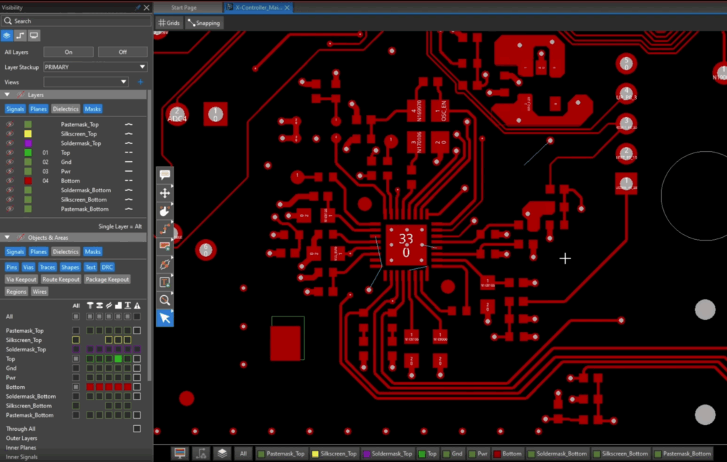
With the increasing reliance on simulation and analysis, comes the responsibility to understand both the capabilities and the limitations of these tools. While able to calculate remarkably accurate results, they do rely on some basic assumptions. Not long ago, “the VIA” was assumed to be a plated hole running the full thickness of the circuit board, resembling a coaxial cable, and could be sufficiently modeled as such. The drive for miniaturization and advances in manufacturing revolutionized this structure, introducing laser drilling, buried and blind, nested, and stacked constructs which quickly invalidated our coaxial cable model. Now they can be modeled in detail, using 3D solvers. Design teams, likely aided by simulation, recognized the via as the single structure in the signal path that presented both the greatest threat to signal integrity and the largest contributor to discrepancies between simulation and measurement. Had we not challenged the assumptions made regarding the VIA, when they no longer held true, simulation and measurement would have continued to diverge as the complex via structures became mainstream. Instead, traditional simulation, aided where necessary with 3D Electro-Magnetic Solvers continues to produce results very predictive of the actual measured product.
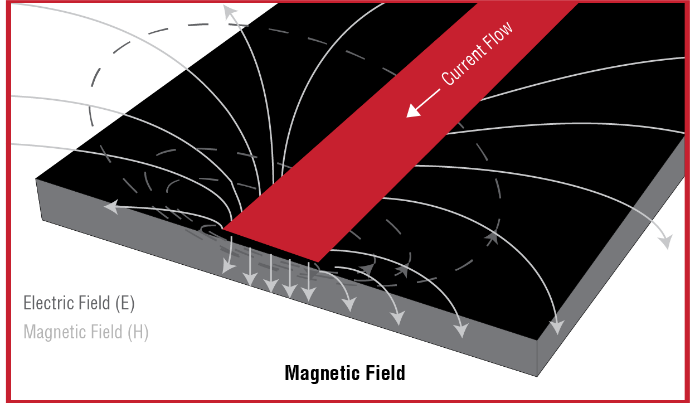
The ability to study, sweep, optimize, rinse, and repeat every physical parameter, such as trace width, via size, and material property of any (or every) structure in a signal’s transmission path has enabled a virtual explosion in data throughput. Where we once struggled moving from 2.5 GHz to 3.125 GHz, we now leap from 5 GHz to 40 GHz gig in a single product generation. This intensive, microscopic almost hyper-focused examination of each and every element along a signal path has enabled the throughput advances needed to enable the technologies such as 5G, high-definition video, and more. It has also exposed one of the most fundamental principles, electricity flows in a loop. In fact, every electron that rocketed down our meticulously groomed signal path, must return to complete the loop.
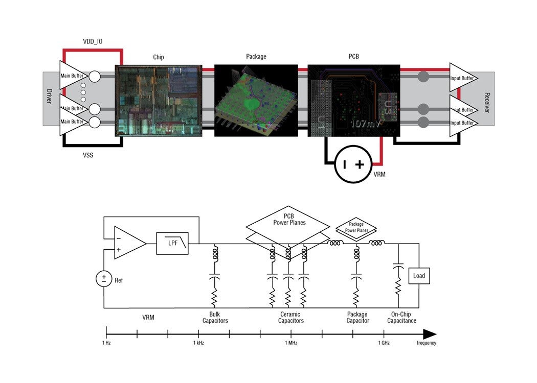
New Problems – Measuring the Whole Loop
Not unlike the “via assumption” (which served its purpose well until modern constructs rendered it obsolete), many signal integrity solutions utilize a “ground assumption”, an idealized model for the return path, assuming an uninterrupted ideal reference. Made up largely of power and ground planes, the “return” has historically been modeled as continuous copper and had very little effect on a signal’s fidelity. Also like the Via, the power and ground planes, have undergone significant change in their composition on many modern circuit boards. Shared voltage layers, often with substantial voids due to anti-pads and isolation areas, as well as the multi-layer nature of the power/ground routing today, has again put us in a situation where the assumptions made within the simulation environment may not reflect the conditions seen on the actual, constructed board.
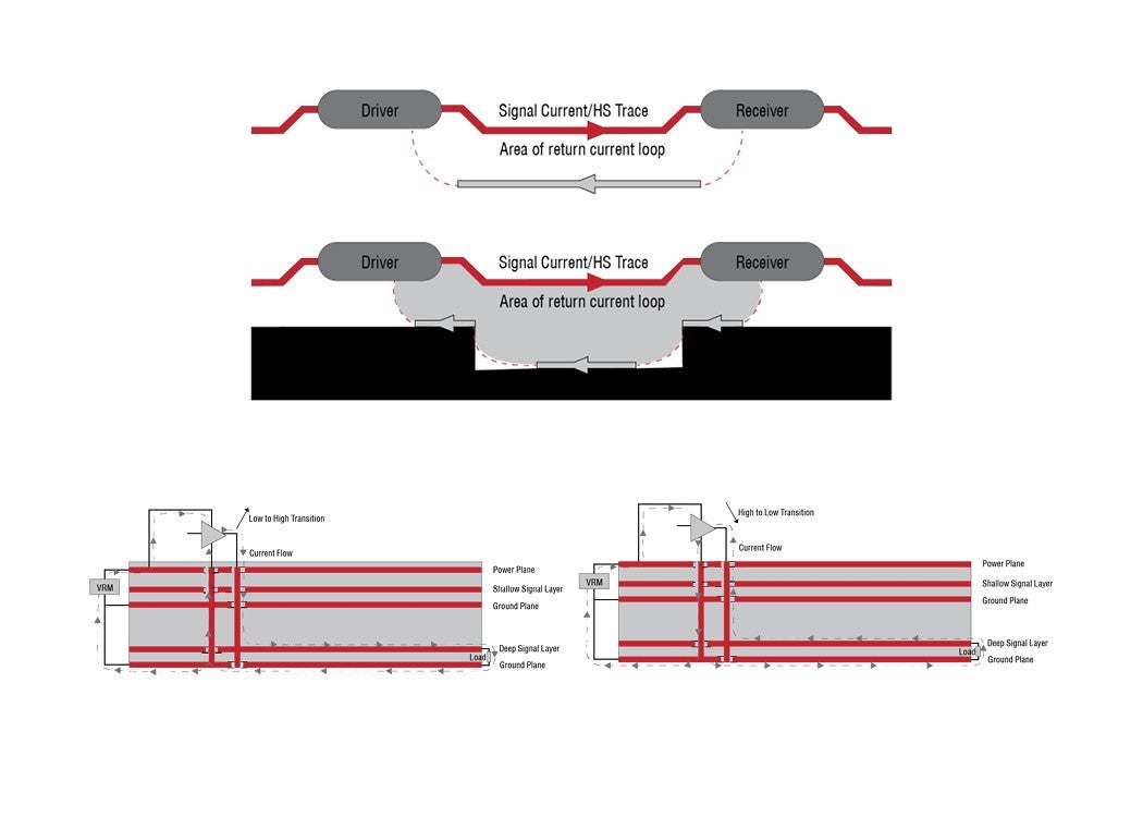
Further complicating this is the variability in the path itself. While most routed signals follow an intuitive route from pin-to-pin, the return is much more complex, often containing numerous connections and redundancies. The actual route of the returning current can be difficult to establish as it is highly influenced by inductive forces directing current flow to the path of least impedance (not necessarily the shortest point-to-point distance). Furthermore, the returning current will change its route with frequency making the structural, model by element, approach used for the outgoing signal nearly impossible.
Enter Power Integrity for PCB Designers
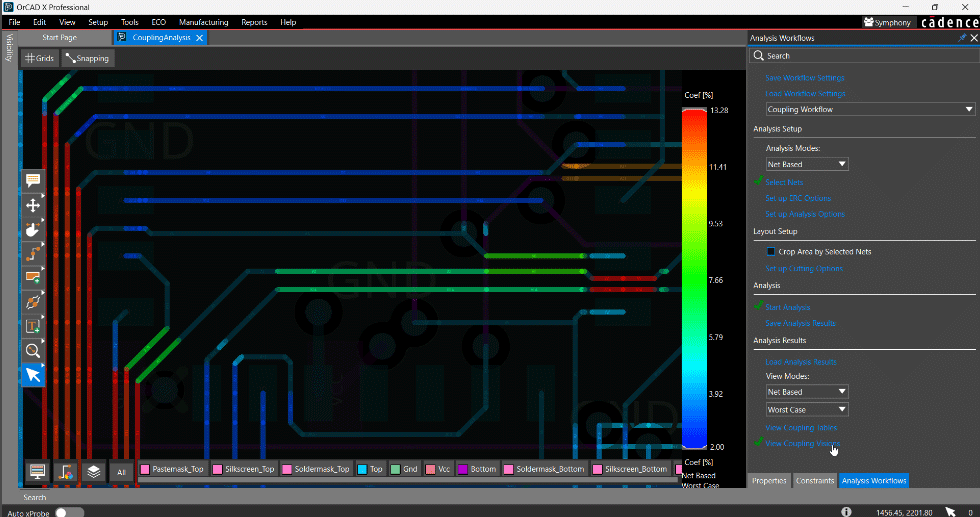
Fortunately, much like we use the 3D solver to overcome via challenges, power integrity (PI) offers a solution for return path and power management. PI can be used (like the solver for vias) for the purpose of creating a detailed model of the power and ground system, or Power Distribution Network (PDN).
Power-aware, signal integrity simulation with integrated 3D EM modeling represents the pinnacle of the electrical simulation market today. Phrases like “virtual prototype” and “digital twin” are used largely and without exaggeration to describe the accuracy achievable with these tools in the proper hands. The combined technologies, SI, PI, and 3DEM are driving the high-speed elites and enabling the speeds and performance that are creating new markets. While collectively they can be used to predict a product’s behavior without building, it is not an all or nothing gain. There are tremendous incremental benefits in each area as simulation understanding grows. Much has been written in the signal integrity space and its virtues are well accepted. Power integrity, by comparison, is a relative newcomer and its usage and value are not as widely known. The benefits associated with visualizing both power noise and signal noise simultaneously when making signal quality measurements is straight forward and a desirable goal but may require greater effort than is necessary for every signal.
An intermediate approach may be to use power integrity and signal integrity tools independently. Power analysis can ensure the power and ground system providing the return path meets predefined requirements. Signal Integrity analysis can then proceed with confidence knowing any deviation from the assumed “perfect” return path, native in the tools, will be bounded and predictable based on the PI results. Additionally, PI can ensure the full supply voltage and therefore the same voltage swing being simulated, is available to even the farthest chip from the supply.
Solving the Power Problem
Conceptually, creating a functional power delivery network is easy, simply provide a continuous copper path from power source to each load capable of supplying adequate current at a steady voltage and an uninterrupted, continuous return path for each switching signal. The difficulty is not in the complexity, but rather the enormity. Multiple voltage requirements, rising power consumption, and increasing circuit density are but a few of the challenges facing the power system. Even the simplest products routinely have multiple power domains occupying the same physical space as a single voltage once did. Exacerbated by a relentless drive towards miniaturization, they combine to create a PDN that has evolved to a point where there is just too much for visual inspection to be reliable. With methods in place to ensure quality power delivery, we will shift focus to the secondary, albeit equally vital role of the PDN, return path. Disruptions in the return path, including ground slots and reference layer changes, are fast becoming the most problematic issues seen in the SI community. Often difficult to detect in a lab setting, these troubles originate in the power plane routing, but routinely evade detection as they fall in the area where the SI simulators are assuming conditions that do not reflect the actual PCB.
Going Forward
This series will address problems commonly associated with the power side of system design, discussing how to improve power integrity for PCB designers through simulation in both power delivery and the return path. Ultimately, we hope to encourage design teams to embrace simulation, understand its limitations, and continue to incorporate complementary technologies, like 3D solvers and Power Integrity, to extend their current capabilities. Read the next article in this series Jernberg PI #2: DC Power Delivery Network Analysis.
Contact us for more information on how Sigrity can be used to analyze signal integrity and power integrity for PCB Designers.