Coupling refers to the unwanted transfer of electrical energy from one trace to another. In signal coupling, the signal-carrying trace that generates electromagnetic interference (EMI) and induces unwanted noise onto adjacent traces is referred to as the aggressor while the adjacent trace that is affected by the interference from the aggressor trace is referred to as the victim. Coupling should be evaluated and properly managed to ensure consistent and reliable signal integrity across the board for high-speed designs as unwanted coupling can be detrimental to signal performance.
What is Signal Coupling?
Signal coupling is a phenomenon that occurs when electrical energy is transferred between conductors in close proximity to each other as a magnetic or electric field. Sometimes coupling is desired for circuit operation. For example, in a transformer the secondary coil is induced by a magnetic field generated by the primary coil. However, undesired coupling can occur in any circuit, due to parasitic inductance and capacitance, as well as the changing magnetic field generated when current through a trace or wire changes.
Capacitive Coupling
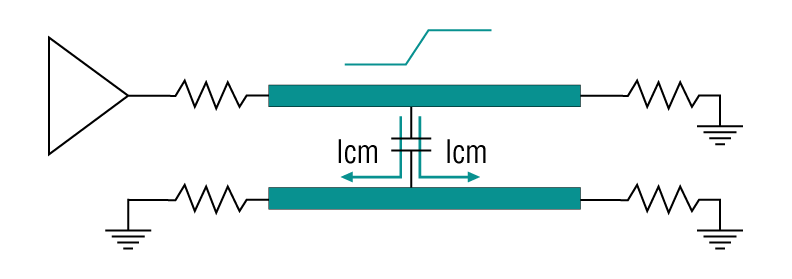
Capacitive coupling occurs when two conductors are close enough that the electric field from one induces a voltage in the other. This is common in closely spaced traces or between traces and ground planes.
Inductive Coupling
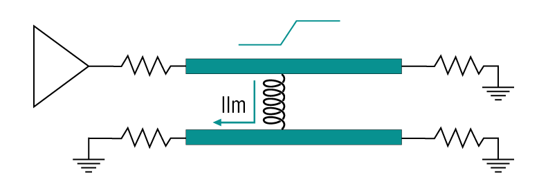
Inductive coupling occurs when a changing magnetic field induces a current in an adjacent trace or loop. This is commonly seen in tightly coupled loop areas or power traces for high-speed signals and power lines.
How to Measure Coupling
Coupling can be measured with the calculation of coupling coefficients which are used to express the strength of all induced coupling on a given trace. The coupling coefficient is dependent on saturation length and the per-unit near-end crosstalk or NEXT. Saturation length refers to the maximum trace length beyond which increasing the length does not significantly affect signal propagation delay, resistance, or attenuation. The saturation length can be calculated with the following equation:
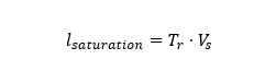
Where:
Tr= Rise Time
Vs= Signal velocity
If the coupled length is greater than or equal to the saturation length, the coupling coefficient is the same as the Near-end crosstalk or NEXT coefficient. Near-end crosstalk can be calculated with the following formula:
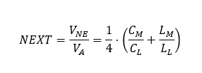
Where:
VNE= Near End Voltage
VA= Aggressor Voltage
CM= Mutual Capacitance
CL= Victim Line Capacitance
LM= Mutual Inductance
LL= Victim Line Inductance
If the coupled length (lcoupled) is less than the saturation length the coupling coefficient can be calculated by:
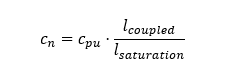
Where:
Cn= Total Coupling Coefficient
Cpu= NEXT Coupling Coefficient
This coupling coefficient can be used to determine how much of the trace is coupled and if any adjustments should be made to minimize unwanted coupling. Corrections should be made for trace lengths with greater than 5% of coupling for the total length of the net. Traces should be reviewed further and adjusted as required for coupling coefficients between 2% and 5% of the total length of the net.
Common Causes of Signal Coupling
Unwanted signal coupling can arise from various factors throughout the PCB layout. The table below will help to identify the cause of coupling, why the PCB feature effects signal quality, and a solution to help PCB designers identify and correct unwanted coupling in their designs.
| Cause | Problem | Solution |
|---|---|---|
| Parallel Trace Routing | When traces are routed too close and in parallel to each other, the electromagnetic fields generated by one trace can induce a signal in the adjacent trace, leading to crosstalk. | Increase trace spacing or incorporate shielding. |
| Differential Pair Imbalance | In differential signaling, an imbalance in trace lengths or spacing can reduce the effectiveness of noise cancellation. | Optimize differential signaling. |
| Signal Coupling Between Layers | Improper or insufficient placement of ground planes can create poor isolation between layers and allow signals on one layer to couple with signals on another. | Optimize the layer stackup and develop a routing strategy. |
| Long Trace Lengths | Long traces act as transmission lines and can pick up or radiate noise, leading to coupling with other traces or components. | Develop a routing strategy. |
| Impedance Variations | Variations in trace impedance, caused by changes in width, spacing, or proximity to other traces or planes, can lead to unwanted coupling. | Implement controlled impedance. |
Understanding Impacts from Signal Coupling
Signal coupling can affect overall system performance and have several negative effects on signal quality including the following common signal integrity issues:
- Noise
Noise refers to any unwanted electrical interference that distorts or disrupts the original signal. With coupling, noise can be seen through the transfer of energy from the aggressor trace onto the victim trace.
- Increased Signal Delay and Skew
Coupling can cause variations in propagation time for signal transmission- specifically signal delay and skew. This can disrupt the synchronization of high-speed circuits and effect circuit reliability.
- Increased Crosstalk
Signals in close proximity to each other can transfer energy, causing noise or crosstalk.
- Bit Errors
In digital circuits, coupling can cause bit errors by distorting signals. This may lead to incorrect data being processed or transmitted.
- Signal Corruption
Signals can become corrupt due to unwanted coupling. Signal corruption refers to the distortion, degradation, or unintended modification of electrical signals as they travel through traces resulting in data errors, poor signal integrity, and malfunctioning circuits.
To prevent these issues, PCB designers must try to minimize unwanted signal coupling through mitigation strategies.
Mitigation Strategies for Signal Coupling
Unwanted signal coupling must be addressed to improve signal quality in your PCB designs, ideally throughout the PCB design process when change is easiest to implement. To correct unwanted coupling, the following strategies can be utilized:
1. Implement Trace Spacing
Since the transfer of energy occurs between traces within close proximity to each other, the most common mitigation strategy to reduce unwanted coupling is to increase the spacing between traces. This is especially important for high-speed signals and sensitive traces. A good rule of thumb is to increase trace spacing to be 3x the trace width distance between the victim and aggressor traces.
- Increase Separation Between Sensitive Traces
- Implement Trace Spacing 3x the Trace Width Distance
2. Optimize the Layer Stackup
Optimize the PCB layer stackup to isolate sensitive signals and provide effective grounding. Solid ground and power planes should be used in the design to provide low impedance return paths and reduce coupling.
- Use Solid Ground and Power Planes
- Isolate Sensitive Signal Layers
3. Incorporate Shieding
Use shielding techniques, such as ground shields or guard traces, to protect sensitive signal paths from coupling. Placing a grounded guard trace between signals can block crosstalk. Vias can also be used as a shield to protect sensitive circuitry and signals.
- Use Guard Traces
- Incorporate Via Shielding
4. Incorporate Controlled Impedance
Design traces with controlled impedance to minimize reflections and signal degradation. Some software solutions will help you determine the trace specifications, such as width and spacing, to achieve your desired impedance based on the stack up configuration. These parameters can then be configured as rules in the design to ensure the desired impedance is achieved throughout the PCB layout. Impedance requirements will vary based on the technology and devices used in the design. Impedance analysis can also be performed to verify continuity and improve signal integrity.
- Determine Impedance Requirements
- Implement Controlled Impedance for Critical Signals and Technology
5. Optimize Differential Signaling
Using differential pairs for high-speed signals can improve noise immunity and reduce coupling effects. Keep differential pairs tightly coupled to minimize external noise. Utilize software features to ensure proper differential signaling such as rules or constraints to configure differential pairs. Constraining differential pairs will ensure signals remain balanced and noise canceling remains effective by configuring parameters including line width, primary gap, neck width, neck gap, gather control, maximum uncoupled length, tolerance, and more.
- Implement Differential Signaling
- Define Rules to Ensure Tight Coupling
6. Implement a Routing Strategy
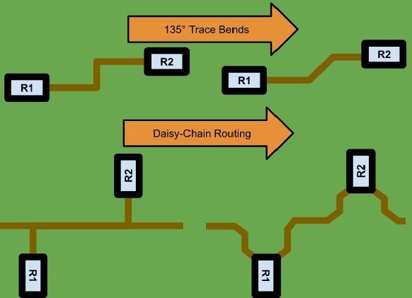
Implementing a routing strategy for your PCB design can help minimize unwanted coupling. Within this routing strategy, it is important to minimize parallel routing between sensitive traces and traces on adjacent layers. Additionally, high-speed or noisy signals should be routed far from sensitive signals or even on differing layers in the PCB design. Keep connections short to minimize the likelihood of coupling.
- Route High-Speed and Sensitive Signals on Different Layers
- Keep Connections Short
- Avoid Routing Sensitive Traces in Parallel
- Route Traces on Adjacent Layers Orthogonally
Implementing these mitigation strategies throughout the PCB design process can result in many benefits and allow you to set the design up for success. But identifying unwanted coupling in the design may be difficult and time-consuming which leads to the question- how do you know when and where to deploy these mitigation strategies?
Incorporating Simulation
To identify where additional mitigation is needed in your PCB design, simulation can be deployed to quickly pinpoint unwanted signal coupling. Simulation tools typically calculate and validate coupling based on the PCB layout and automatic calculations of saturation length and near-end crosstalk. Simulation can be used to analyze signal integrity and identify unwanted coupling created by:
- Insufficient trace spacing
- Parallel routing between layers
- Long trace lengths
Once these issues are identified, mitigation strategies can be incorporated into the PCB design to reduce unwanted coupling and, in turn, improve signal integrity.
Why Should You Analyze Coupling?
Implementing mitigation strategies for unwanted signal coupling and performing coupling analysis not only improves the performance of your PCB designs but also helps you adhere to the project requirements and timeline. Performing coupling analysis can benefit your PBC design process by:
- Improving Signal Quality
Performing coupling analysis will minimize unwanted interactions between signal traces and improve signal integrity for both analog and digital circuitry:
- Digital Circuits: Coupling can cause bit errors by distorting signals. Correcting coupling will ensure correct data is being processed or transmitted.
- Analog Circuits: Coupling can result in signals becoming corrupted. Correcting coupling will improve accuracy and reliability of the design.
- Minimizing Crosstalk
Coupling analysis identifies the unwanted transfer of signals between adjacent traces, allowing you to mitigate crosstalk and ensure reliable signal transmission.
- Improving Reliability
Coupling can cause variations in signal propagation times (signal delay and skew), which can disrupt synchronization of high-speed circuits. Reducing unwanted coupling improves signal reliability and produces accurate signal transmission.
- Preventing Ground Bounce and Noise
In high-speed digital circuits, ground bounce, or voltage fluctuation in the ground plane, is often caused by simultaneous switching of signals. Common strategies for mitigating coupling such as incorporating solid ground planes and via stitching are also strategies for minimizing ground bounce and preventing noise.
- Reducing Troubleshooting Time
The cause of signal integrity issues can be hard to pinpoint in the lab, leading to a cycle of designing, testing, and fixing that can push your project timeline out. Analyzing unwanted coupling through simulation will help you pinpoint issues quickly and improve signal quality before prototyping or production.
Performing coupling analysis at any stage of the design is going to yield benefits but having this as the last step in your design process can result in late-stage design changes, additional rework, and more design hours if any issues are found. Analyzing coupling throughout the PCB layout will allow you to find and correct unwanted signal coupling while you are designing- this is where Sigrity Aurora can help.
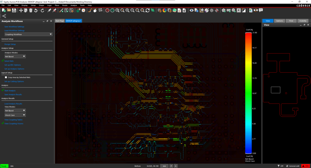
Identifying Signal Coupling with Sigrity
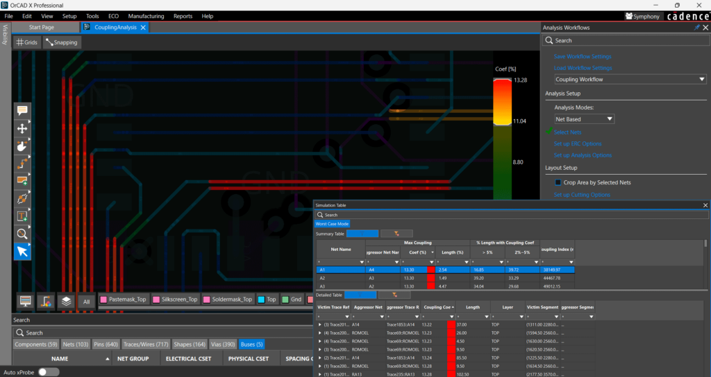
Sigrity Aurora includes easy-to-use workflows that step you through the required procedure to analyze signal and power integrity in your PCB designs. The Coupling Workflow in Sigrity Aurora is most commonly used to identify unwanted signal coupling in the PCB design, providing a step-by-step procedure to perform layout-based coupling analysis directly within the PCB layout canvas. The coupling workflow can be used by PCB designers throughout the PCB layout process to identify and correct issue when change is easiest, reducing time spent on prototyping, troubleshooting, and redesigning the PCB. Sigrity Aurora streamlines the product development process and allows you to efficiently analyze signal coupling with:
- A unified environment for PCB design and signal integrity analysis
- Easy-to-use workflows
- Minimal setup and modeling
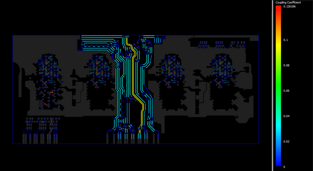
- Visual overlays directly on the PCB canvas with color-coded results
- Detailed, tabular results to easily pinpoint unwanted signal coupling
Learn more about signal coupling and how to resolve issues using Sigrity Aurora with our free course: Introduction to In-Design SI/PI analysis with Sigrity Aurora.