Impedance refers to the opposition that a circuit or trace offers to the flow of signals which is influenced by factors such as trace width, height above the ground plane, dielectric material, and frequency of the signal. Impedance should be evaluated and properly managed to ensure consistent and reliable signal integrity across the board for high-speed, RF, and mixed-signal designs as discontinuities in impedance can be detrimental to signal performance.
What Are Impedance Discontinuities?
Impedance discontinuities are abrupt changes in the impedance along a signal path. These changes cause signal reflections and distortions, which can degrade signal integrity and lead to communication errors or data loss.
Common Causes of Impedance Discontinuities
Impedance discontinuities can arise from various factors throughout the PCB layout. The table below will help to identify the cause of the impedance discontinuity, why the PCB feature disrupts impedance, and a solution to help PCB designers identify and correct impedance discontinuities.
| Cause | Problem | Solution |
|---|---|---|
| Changes in Trace Width | Variations in the trace width can result in changes to impedance, such as necking down a trace to route through tight spaces. | Keep trace geometry uniform. |
| Via Transitions | When a signal changes layers through a via, the impedance can change due to the via’s inductance and capacitance. | Optimize and minimize via usage. |
| Crossing a Split in a Plane | If a trace crosses a gap in the reference ground plane, the lack of a consistent return path can cause impedance changes. | Follow PCB stackup guidelines and incorporate simulation. |
| Via Stubs | At high frequencies, the unused portion of vias or stubs can act as resonant structures and contribute to impedance discontinuities. | Incorporate backdrilling to remove unused portions of vias. |
| Trace Corners and Bends | Sharp bends in traces can cause a change in the effective trace width and length, leading to impedance discontinuities. | Develop a routing strategy to reduce impedance discontinuities. |
| Connector Interfaces | When signals transition between the PCB and external connectors, like USB ports, differences in impedance can cause discontinuities. | Implement impedance matching and termination strategies. |
Understanding Impacts from Impedance Discontinuities
Impedance discontinuities can affect overall system performance and have several negative effects on signal quality including the following common signal integrity issues:
- Signal Reflections
When impedance is mismatched, part of the signal is reflected back towards the source, causing noise and reducing signal quality.
- Ringing
Reflections cause ringing (where the signal oscillates at the transition edges) which can lead to misinterpretation of the signal.
- Jitter
Reflections can lead to timing variations or jitter in digital signals.
- Overshoot and Undershoot
Mismatched impedance can cause the signal to exceed or drop below its normal levels of operation. This can damage components or cause incorrect logic levels.
- Increased Crosstalk
Signal reflections can interfere with nearby traces, causing noise or crosstalk.
- Data Errors
Degraded signal quality can result in bit errors or communication failures in high-speed systems.
To prevent these issues, PCB designers must try to minimize impedance discontinuities through mitigation strategies.
Mitigation Strategies for Impedance Discontinuities
1. Implement Impedance Matching
Ensure traces are designed with controlled impedance to match the source and load. Many software packages will allow you to configure rules for impedance and automatically check adherence to those rules throughout the PCB layout. If needed, use termination resistors, such as series or parallel termination, to match the impedance and absorb reflection.
-
-
-
-
- Design for Controlled Impedance
- Include Proper Termination
-
-
-
2. Develop a Routing Strategy
Impedance can be disrupted with abrupt changes in the traces or connections on the PCB. Maintain uniform impedance by keeping trace width and thickness the same. Avoid making sharp bends when routing and instead opt to use smooth curves with 45° bends instead. Try to avoid stubs or branches, especially when routing high-speed signals. Stubs or unused/unconnected traces branching off from a signal path can create impedance mismatches and reflections.
-
-
-
-
- Deploy Uniform Width and Thickness
- Avoid Sharp Bends
- Minimize Stubs
-
-
-
3. Follow PCB Stackup Guidelines
The stackup and materials used in the construction of the PCB are going to have a direct effect on the impedance. Use PCB materials with consistent dielectric properties to maintain uniform impedance. For designs with controlled impedance, be sure to provide detailed information to your manufacturer and allow for minor adjustments to the stackup, trace width, and trace spacing to meet your impedance requirements.
-
-
-
-
- Use Controlled Dielectric Properties
- Allow Manufacturing Adjustments
-
-
-
4. Optimize Via Usage
Via transitions will affect the impedance of traces; therefore, you should avoid using an excessive number of vias, especially in high-speed signal paths. If vias are necessary, incorporate backdrilling to remove unused portions and prevent reflections.
-
-
-
-
- Reduce Via Transitions
- Use Backdrilling
-
-
-
Incorporating Simulation
To identify where additional mitigation is needed in your PCB design, simulation can be deployed to quickly pinpoint impedance problems. Simulation tools typically calculate and validate impedance based on the trace layout, stack-up, and material properties. Simulation can be used to analyze signal integrity and identify impedance discontinuities created by:
- Changes in trace widths
- Via transitions
- Crossing a split in the plane
- Via stubs
Once these issues are identified, mitigation strategies can be incorporated into the PCB design to improve impedance and, in turn, signal integrity.
Why Should You Analyze Impedance?
Implementing mitigation strategies for impedance discontinuities and performing impedance analysis not only improves the performance of your PCB designs but also helps you adhere to the project requirements and timeline. Performing impedance analysis can benefit your PBC design process by:
- Improving Signal Quality
Improve the quality of signal transmission by reducing common signal integrity issues including signal reflections, ringing, jitter, overshoot, undershoot, and crosstalk.
- Improving Timing and Data Quality
Impedance mismatches can cause different signal paths to have different delays. This signal skew is problematic in systems where timing synchronization is critical, as it can cause:
- Bit errors and increased error rates
- Data corruption
- Degraded eye diagrams
- Reduced signal clarity
Analyzing impedance upfront will help ensure proper timing and improve the quality of data transmission.
- Reducing Component Stress and Failure
Overshoot and undershoot can cause electrical overstress on components and can result in premature failure or degraded component performance. Analyzing impedance and improving signal integrity can reduce the risk of component failure, improving PCB reliability and product lifespan.
- Guaranteeing Adherence to Impedance Requirements and Standards
Many high-speed electronics and devices require specific impedance values to function properly and achieve precise timing. Impedance discontinuities can result in non-compliance to industry standards and communication protocols. Analyzing impedance during PCB layout can help guarantee adherence to industry standards before production.
- Reducing Troubleshooting Time
The cause of signal integrity issues can be hard to pinpoint in the lab, leading to a cycle of designing, testing, and fixing that can push your project timeline out. Analyzing impedance through simulation will help you pinpoint impedance discontinuities quickly and improve signal quality before prototyping or production.
Performing impedance analysis at any stage of the design is going to have benefits but having this as the last step in your design process can result in late-stage design changes, additional rework, and more design hours if any issues are found. Analyzing impedance throughout the PCB layout will allow you to find and correct impedance discontinuities while you are designing- this is where Sigrity Aurora can help.
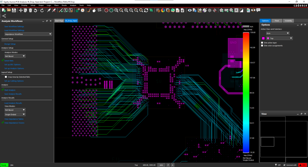
Identifying Impedance Discontinuities with Sigrity
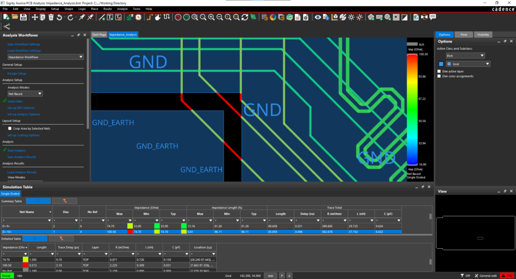
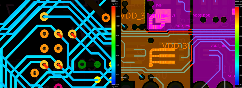
Sigrity Aurora includes easy-to-use workflows that step you through the required procedure to analyze signal and power integrity in your PCB designs. The Impedance Workflow in Sigrity Aurora is most commonly used to identify impedance discontinuities in the PCB design, providing a step-by-step procedure to perform layout-based impedance analysis directly within the PCB layout canvas. The impedance workflow can be used by PCB designers throughout the PCB layout process to identify and correct issue when change is easiest, reducing time spent on prototyping, troubleshooting, and redesigning the PCB. Sigrity Aurora streamlines the product development process and allows you to efficiently analyze impedance discontinuities with:
- A unified environment for PCB design and signal integrity analysis
- Easy-to-use workflows
- Minimal setup and modeling
- Visual overlays directly on the PCB canvas with color-coded results
- Detailed, tabular results to easily pinpoint impedance issues
Learn more about impedance discontinuities and how to resolve them using Sigrity Aurora with our free course: Introduction to In-Design SI/PI analysis with Sigrity Aurora.