Electronic circuit board design is a multi-stage process with the schematic creation and PCB layout being the primary activities. Although each stage has its own set of tasks and objectives, they are intricately linked. And prior to transitioning from one stage to the next, verification is necessary to achieve design efficacy and overall PCB development efficiency.
Verifying your layout, which should include an accurate 3D rendering of your board and elements, is essential to ensure your CM can build your board to reflect design intent and meet operational and reliability goals. Knowing how to review a PCB layout effectively is necessary to satisfy this requirement.
PCB Layout Review: What to Review and Why
Laying out your board can be a complex and time-consuming exercise. Moreover, your design decisions and choices dictate how well or even if your board can be fabricated and assembled. Consequently, it is important to know what to review and why to avoid contingencies like redesign, excessive board spins and unnecessary manufacturing costs.
| PCB LAYOUT REVIEW | |
| What to Review | Why It’s Important |
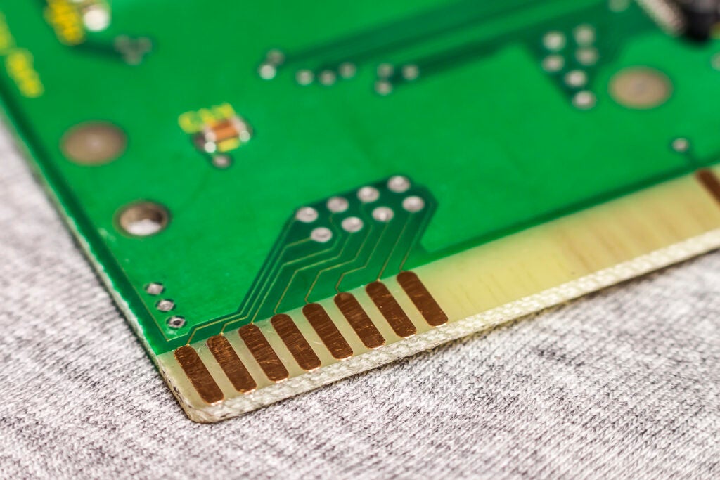
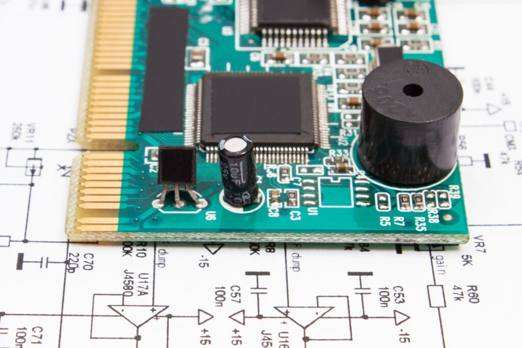
| Component Footprints | Footprints and landing patterns determine the space designated for parts during fabrication etching. Errors here will prevent accurate component placement during assembly and are not fixable with rework. |
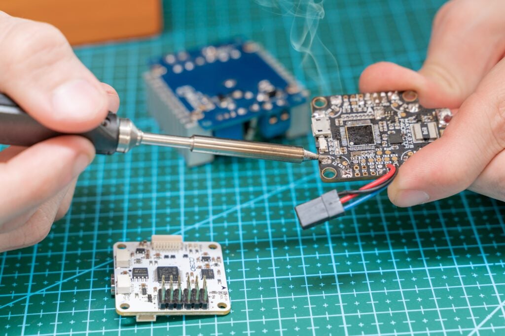
| Component Placement | Most components are placed using an automatic pick and place machine. Locations are based on the layout given in design files, and misalignment can result in soldering failures that will adversely affect operation if not correctable by rework. |
| Trace Routes and Connections | Accurate traces are critical for board operation and performance. Additionally, oversights like unconnected nets and floating pins will likely not be discovered by your CM, and lead to wasted boards and low yield rates. |
| Drill Hole Dimensions | Both plated through holes (PTHs) used for vias and non-plated through holes (NPTHs) used for board mounting and secure installation, must adhere to size, depth and aspect ratio standards. |
| Spacing and Clearances | Spacing and clearance between board elements and the board edge must conform to industry standards. Failing to do so will mean board redesign. |
| PCB Stackup | Multilayer boards, which are becoming more commonplace, require additional considerations; such as layer count and symmetry, via type and placement, grounding strategy and impedance matching across material levels. |
| Labels and Indicators | Silkscreen items, like component labels and reference indicators, are critical elements to ensure parts are placed and oriented accurately. |
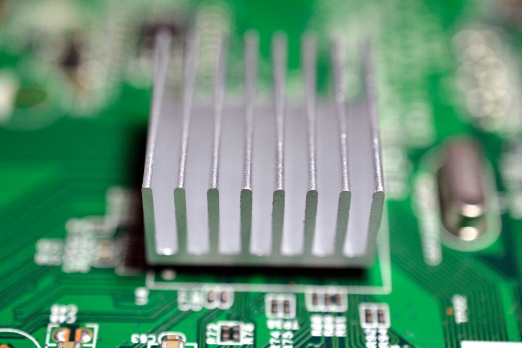
| Power and thermal analyses | To ensure adequate power distribution and heat dissipation–to check thermal vias and heat sink effectiveness for high power components and safety–a thermal review of your board should be performed. |
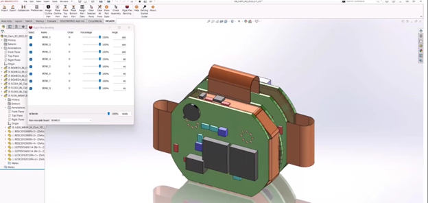
| Final Visual Inspection | Prior to submitting your design for fabrication and assembly, a visual inspection; such as a 2D and 3D rendering or digital twin, should be examined to verify dimensionality and ensure no collision issues for enclosures or MCAD implementation. |
As shown above, it is not simply a good idea, but essential to review a PCB layout before passing it to your CM for manufacturing.
How to Review a PCB Layout Effectively
As mentioned earlier, schematic generation and PCB layout design are separate, yet linked stages. For effective circuit board design, this relationship should be leveraged by performing a comprehensive schematic review before starting your layout design. Subsequently, the PCB layout design stage is simplified. For example, connectivity issues, such as unconnected nets and floating pins, should have been verified and corrected.
For most PCB design software programs today, some degree of ability to review your PCB layout is incorporated. And one of the most important of these capabilities is design rule checking (DRC), which identifies errors based on a set of predefined constraints. Additional functionalities like partial or automatic trace routing and visual inspection of the layout, including internal layers, are also important to ensure that all important aspects of the PCB layout are reviewable.
The availability and utilization of these capabilities, which can be optimized as shown below, directly determines the efficiency of your PCB layout review and board development process.
Optimizing PCB Board Review Efficiency
By following a few simple steps as listed below, you can maximize the effectiveness of PCB layout review, as well as the efficiency of its execution.
- Start with a verified schematic design.
- Acquire and use your CM’s DFM and DFA rules and guidelines to define layout constraints.
- Perform DRC checks often, and correct errors during design when it is simpler and faster to do so.
- Leverage visualization, especially 3D rendering, to inspect layout elements and dimensionality.
The best way to achieve the objectives above is to employ a PCB design software solution; such as OrCAD X Presto, with advanced capabilities for expediting your ability to expeditiously review and verify your PCB layout design.
EMA Design Automation is a leading provider of the resources that engineers rely on to accelerate innovation. We provide solutions that include PCB design and analysis packages, custom integration software, engineering expertise, and a comprehensive academy of learning and training materials, which enable you to create more efficiently. For more information on how to review a PCB layout most efficiently and how we can help you or your team innovate faster, contact us.