Important PCB Design Rules for an Efficient Workflow

PCB design rules provide guidelines that ensure consistency, reliability, and manufacturability throughout the PCB design process. These rules help prevent common design errors, such as inadequate trace widths, improper spacing, and incorrect component placement, that can lead  to signal integrity issues, overheating, or even complete board failure.

By adhering to PCB design rules, designers can streamline the design-build-test (DBT) process, reduce the need for rework and costly revisions, and facilitate easier communication with manufacturers.

Essential PCB Design Rules and Benefits

Designing PCBs can be complex. Consequently, the number of rules that are applicable can seem overwhelming when viewed from a comprehensive perspective. These rules can be more readily evaluated and digested when divided into subcategories, as below.

Component Placement

Design Rules

Benefits

Place components close to their respective connectors

+ Minimizes noise and power loss

✔ Group components by function

+ Minimizes trace lengths and interference

✔ Follow good spacing rules and guidelines between components and other elements

+ Provides adequate room for solder paste application and solder flow to ensure good connections during PCB assembly

✔ Provide heat-generating components with adequate space and add heat sinks and vias, if needed

+ Dissipates heat

Signal Integrity

✔ Maintain adequate spacing between parallel signal traces

+ Reduces crosstalk, especially for high-speed signals

✔ Place guard traces between high-speed or sensitive signals

+ Shields signals from interference

✔ Ensure differential pairs are of equal length to maintain signal integrity and timing accuracy

+ Maintains signal integrity and timing accuracy

✔ Use short trace lengths and optimize impedance matching 

+ Minimizes propagation delay and maximizes signal transfer strength

Trace Routing

✔ Minimize trace lengths

+ Reduces resistance and inductance

✔ Use appropriate trace widths for different signals and power levels, following IPC standards

+ Ensures current capacity and signal integrity

✔ Maintain consistent trace width and spacing for high-frequency signals

+ Controls impedance and reduces signal reflections

Power and Ground

✔ Use a continuous ground plane

+ Reduces noise and provides a return path for signals

✔ Separate analog and digital ground planes

+ Minimizes noise interference between sensitive analog components and digital signals

✔ Place decoupling capacitors near power pins of ICs 

+ Filters out noise and stabilizes power supply

Electromagnetic Compatibility
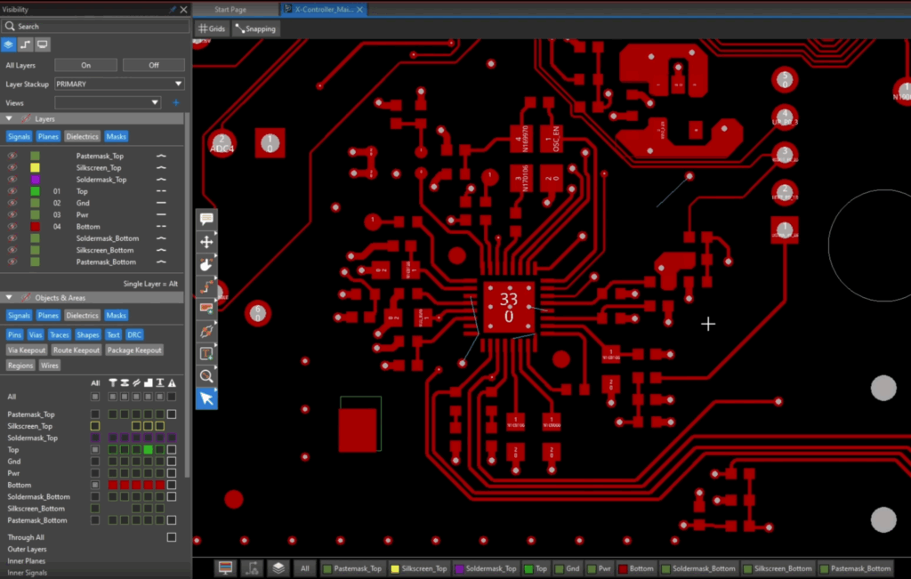
Reduce loop area for high-speed signals

+ Minimizes electromagnetic interference (EMI)

✔ Apply shielding techniques like ground planes, guard traces, and enclosures

+ Mitigates EMI

Design Rule Checks

✔ Set clear design rules in the PCB design software

+ Automatically checks for issues like trace width, spacing, and clearance during the design process

✔ Run DRC during the design process to catch and correct errors early

+ Ensures compliance with manufacturing capabilities and design standards

✔ Maintain adequate clearance and creepage distances between traces

+ Prevents arcing and ensures safety.

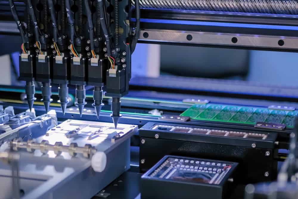
Design for Manufacturability

✔ Ensure that vias and through-holes have adequate annular rings 

+ Avoids manufacturing issues

✔ Adhere to manufacturing capabilities for minimum trace and space widths

+ Ensures reliable fabrication

✔ Add fiducial marks on the PCB 

+ Assists with automated optical inspection and assembly processes

Testing and Debugging

✔ Incorporate test points for critical signals and power lines 

+ Facilitates testing and debugging of the PCB

✔ Ensure the design accommodates design for in-circuit tests by providing access to nodes for probe contact during testing

+ Enables detection and diagnosis of manufacturing defects and component failures at an early stage

Documentation

✔ Provide documentation on the layer stackup 

+ Assists with manufacturing and ensures design intent is met

✔ Ensure the bill of materials (BOM) and assembly drawings are clear and complete 

+ Avoids miscommunication and errors during the assembly process

Save Time and Money With a Streamlined PCB Design Workflow 

These PCB design rules ensure a smooth design workflow, saving time and money as well as ensuring a quality final product. An efficient PCB design workflow provides the following advantages:

  • Reduces Time-to-Market: Streamlined processes shorten development cycles, allowing products to reach the market faster and gain a competitive edge.
  • Minimizes Errors and Rework: Standardized guidelines and best practices help prevent common design mistakes, reducing the need for costly and time-consuming revisions.
  • Lowers Costs: Optimized use of materials and resources results in significant cost savings.
  • Enhances Quality: Consistent adherence to design rules ensures high-quality PCBs that meet performance and reliability standards.
  • Improves Collaboration: Clear guidelines and efficient processes foster better communication and coordination among design, engineering, and manufacturing teams.
  • Increases Productivity: Efficient workflows streamline tasks and reduce redundant work, boosting productivity and efficiency.
  • Facilitates Scalability: Well-defined workflows make it easier to scale up production and manage larger, more complex projects effectively.

An efficient workflow produces higher-quality PCBs that meet performance standards and reliability requirements, boosting business success. You’ll need to partner with an industry expert who can assist you in effectively implementing these PCB design rules. With decades of industry expertise, EMA Design Automation is ready to help you with the tools, service, and support you need to meet your design goals.

EMA Design Automation is a leading provider of the resources engineers rely on to accelerate innovation. We provide PCB design and analysis packages, custom integration software, engineering expertise, and a comprehensive academy of learning and training materials. For more information on the benefits of PCB design rules and how we can help you or your team innovate faster, contact us.

EMA Design Automation