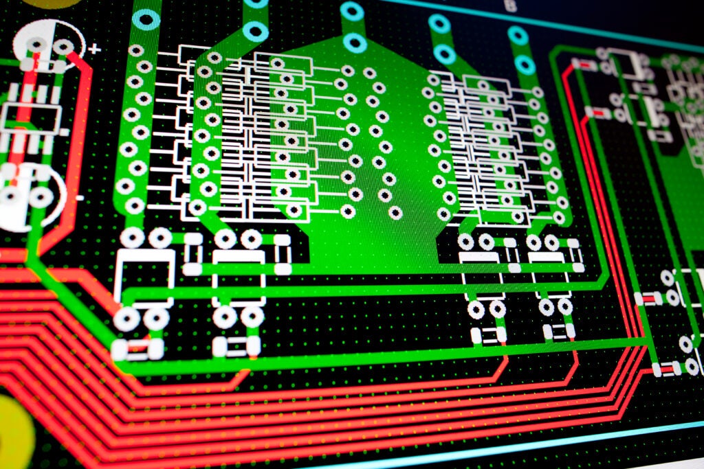
Standard PCBs are the workhorses of the electronics world—reliable, affordable, and suitable for simpler designs. They use thicker lines, through-hole vias, and fewer layers, resulting in larger boards. High-density interconnect (HDI) PCBs, on the other hand, are high-tech athletes—thinner, lighter, and ideal for getting maximum functionality in tight spaces. They achieve this with laser-drilled microvias, blind and buried vias, and more layers, but this complexity comes with challenges, such as signal and power integrity issues. To fully address these challenges, engineers should follow robust HDI PCB design guidelines.
HDI PCB Design Guidelines for Signal and Power Integrity
Signal and power integrity issues in HDI PCB design primarily stem from these advanced circuits’ high density and complexity. With closely packed traces and components, signal integrity challenges include increased crosstalk, electromagnetic interference (EMI), and reflections, which can degrade signal quality and cause data errors. Power integrity issues arise due to the difficulty in maintaining a stable power distribution network (PDN) in such a compact layout, leading to potential voltage fluctuations, noise and excessive energy loss. Microvias and multiple layers complicate these issues, as they require careful management of impedance, return paths, and decoupling strategies to ensure reliable performance.
Here are robust HDI PCB design guidelines to ensure good signal and power integrity.
|
HDI PCB Design Guidelines for Signal and Power Integrity |
|
|
Aspect |
Guidelines |
|
Controlled Impedance |
Ensure trace impedance is controlled and matched to source and load to minimize reflections. |
|
Keep high-speed signal traces short and direct; use 45-degree bends instead of 90-degree angles to reduce impedance discontinuities; route differential pairs together with consistent spacing. |
|
|
Layer Stack-Up |
Design a proper layer stack-up with solid reference planes (ground and power) to reduce EMI. |
|
Return Paths |
Place decoupling capacitors close to power pins to filter out high-frequency noise. Use a mix of capacitance values to cover a wide frequency spectrum |
|
Terminations |
Use proper termination techniques (series or parallel) to match impedance and prevent signal reflections. |
|
Power Distribution Network |
Design an efficient PDN with low impedance across a wide frequency range to provide stable power delivery. |
|
Power Planes |
Use solid power and ground planes to reduce impedance and provide a stable voltage reference. |
|
Via Distribution |
Distribute vias evenly to connect power and ground planes, ensuring a low-impedance path. |
|
Power and Ground Layout |
Minimize the distance between power and ground planes to increase capacitance and reduce noise. |
|
Microvias |
Utilize microvias to connect multiple layers and achieve higher density without compromising integrity. |
|
Aspect Ratio |
Maintain an optimal aspect ratio for vias to ensure reliability and manufacturability. |
|
Advanced Materials |
Use materials with higher performance characteristics to handle increased density and complexity. |
|
Thermal Management |
Implement effective thermal management strategies to address heat dissipation challenges. |
|
Analysis Tools |
Utilize SI/PI analysis tools during the design phase to simulate and validate the board’s performance. |
|
Manufacturing Capabilities |
Ensure your manufacturing partner has the capability and experience to handle HDI technology, including the precision for microvias and fine traces. |
These guidelines help achieve optimal power and signal integrity in HDI PCB design, ensuring reliable and efficient performance for high-density and high-performance electronic applications.
EMA Can Help with HDI PCB Design
Due to their advantageous features, increasingly compact and miniaturized HDI PCB designs will continue to replace standard PCB designs. With OrCAD X Presto PCB design software, HDI boards can be designed with advanced routing and component placement features. As a preferred Cadence Channel Partner, EMA has decades of experience providing the software, training and support–in-house, on-site and remotely–to help you meet and exceed your PCB design objectives.
EMA Design Automation is a leading provider of the resources that engineers rely on to accelerate innovation. We provide solutions that include PCB design and analysis packages, custom integration software, engineering expertise, and a comprehensive academy of learning and training materials, which enable you to create more efficiently. For more information on HDI PCB design guidelines and how we can help you or your team innovate faster, contact us.
