|
ADDITIONAL FPGA PCB DESIGN GUIDELINES |
|
|
Switching Signal Noise (SSN) |
|
|
Decoupling |
|
|
Stackup |
|
FPGA PCB Design Guide Breakdown
Avoiding Discontinuities
Continuity generally refers to the direct connection between signals defined by the netlist. The unrouted connections that appear in a design rule check are not the focus, but rather impedance discontinuities. Any signal traversing a physical medium can experience impedance discontinuities (think routing over split gaps in reference planes, changes in substrate materials, etc.) and are either inductive or capacitive relative to the originating signal characteristics:- Inductive discontinuities appear over-terminated relative to the driver.
- Capacitive discontinuities appear under-terminated relative to the driver. This type of discontinuity can occur when components are in line with the transmission.
- As a first rule of thumb, determine if a via is necessary. Some areas of the board (like under the BGA) require vias for signal breakout. However, careful placement and routing can eliminate unnecessary vias, with the added benefit of reducing cost/fabrication defect vectors.
- Speaking of via breakout, microvias (i.e., blind vias for BGAs) exhibit less of a discontinuity than traditional vias. While they will be more expensive, they are indispensable for HDI boards.
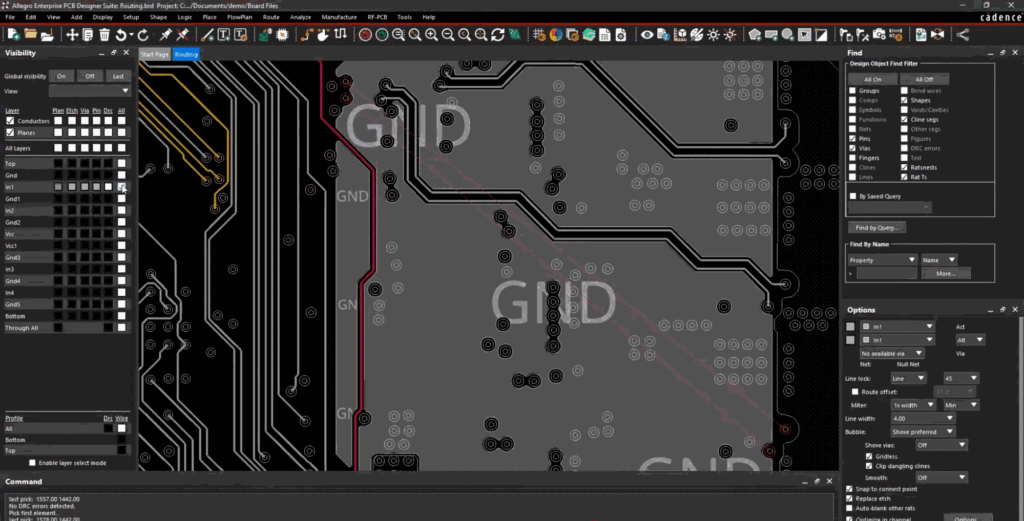
- When routing differential pairs, place a ground via for each via transition equidistant from the transmission line vias. This placement will keep return loops small and limit EMI.
- Consider backdrilling to remove via stubs. This process is optional but can remove unnecessary transmission line length from the via barrels that cause reflections.
Termination
Signals need termination to ensure the correct transfer from driver to receiver in the transmission line and prevent reflections. Placement of the terminating resistors and their topology is key:- Series termination is on the driver-side of the transmission line and is suitable for clock signals only. The terminating resistor acts as a voltage divider for the signal originating at the driver before reflecting from the terminating resistor to the receiver for the full amplitude.
- Parallel termination can be on both ends or only the receiver side of the transmission line. The terminating resistors should be as close to the driver or receiver as possible.
Trace Layout
Accommodating an HDI layout requires tightly coupled traces. Tight coupling reduces the space between traces for greater routing efficiency, but designers must be mindful of crosstalk. Traces should also be as wide as possible to reduce resistive losses during transmission. The 3W rule is an excellent rule of thumb for balancing trace thickness and gaps: measured trace center-to-center, the gap between traces should be at least three times the thickness of the traces. Consider some additional trace guidelines:- Keep skew to a minimum (i.e., zero) for differential pairs to prevent timing mismatches that undermine the common-mode noise cancellation. Although there will be an impedance mismatch where the traces separate to add length to the shorter line, this effect is negligible for all but the shortest differential pair trace lengths.
- Avoid interplanar coupling/crosstalk by having traces cross perpendicular on adjacent signal layers.
EMA Accelerates PCB Designs
FPGA PCB design guides focus on the broad strokes of board development and layout, but individual design intent may supersede these general rules. If you’re looking for support on your next FPGA-enabled device, EMA is here to help. With library support, next-generation layout software, training courses, and additional resources, EMA can streamline electronics development to enable faster design turnaround and better performance.
EMA Design Automation is a leading provider of the resources that engineers rely on to accelerate innovation. We provide solutions that include PCB design and analysis packages, custom integration software, engineering expertise, and a comprehensive academy of learning and training materials, which enable you to create more efficiently. For more information on PCB design documentation and how we can help you or your team innovate faster, contact us.
