Renowned physicist and chemist, Michael Faraday, is often referred to as the “Father of Electromagnetism.” This moniker is well-deserved as Faraday is credited with discovering induction. This phenomenon occurs when a current is created or “induced” in a conductor due to being in close proximity to a magnetic field. This revolutionary discovery significantly advanced our understanding of electricity and magnetism and is the foundation for the invention of many products that we use today, such as electric transformers, electric motors and wireless phone chargers.
The use of devices that leverage electromagnetism is the catalyst for the continuing growth of portable wireless products. However, the magnetic fields generated by these products can have effects that must be considered and addressed. Especially, on and around PCBs, where conductors and radiating components may be in close proximity. The most important issues are electromagnetic interference (EMI) and electromagnetic compatibility (EMC). By employing good EMC analysis tools, you can ensure your RF boards will reliably achieve your performance objectives and minimize any adverse effects.
EMI and EMC
An understanding of the relationship between EMI and EMC, which is defined below, is the first step in designing your PCB or system to minimize the adverse effects of magnetic fields.
As indicated above, EMI and EMC are interrelated. From a design perspective, minimizing EMI translates into better EMC. Consequently, the capabilities necessary and tools implemented to achieve EMC, include targeted EMI solutions.
EMC Analysis Tools: The Best Capabilities
As previously mentioned, multiple sources may impact EMC. Consequently, industry-leading EMC analysis tools, listed below, include capabilities that focus on different root causes.
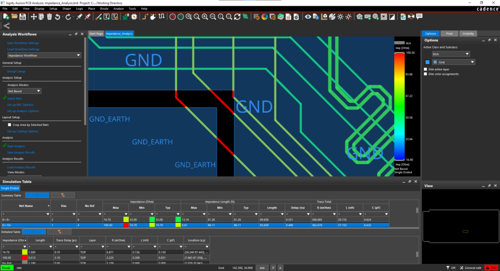
One of the major causes of EMI on PCBs is created as on-board components generate and process RF signals. Consequently, RF simulation software is often applied to address crosstalk, noise reduction, high-speed impedance mismatch, mixed signal interference and other signal integrity issues. Depending on your board’s performance objectives and operational environment, the best solution may require both a targeted EMC analysis tool and a broad EMI-EMC perspective.
Achieving EMC Optimized PCB Design
The trends toward more compact systems with more robust capabilities, as well as expanding applications for electronics-based systems, will only serve to greater crystallize the need for effective EMC analysis tools. Selecting the best tool and implementing it to maximize EMC requires guidance. The steps below can be helpful for maximizing the benefits of your EMC solution.
Guidelines for EMC Analysis Tool Optimization
- Identifying and prioritizing the sources of EMI for your design
- Choose an EMC analysis tool that:
- Targets the most significant source of EMI for your design
- Integrates with your PCB design software
- Is scalable
- Implement a HW testing solution, if necessary
For some designs, the emissions levels demand that a hardware solution, like shielding, is used. In many RF PCB design cases; however, coupling signal integrity analysis design solutions with the best EMC analysis tool for your project will result in an optimized design that satisfies your performance and operational objectives.
EMA Design Automation is a leading provider of the resources that engineers rely on to accelerate innovation. We provide solutions that include PCB design and analysis packages, custom integration software, engineering expertise, and a comprehensive academy of learning and training materials, which enable you to create more efficiently. For more information on how to maximize the benefits of EMC analysis tools and how we can help you or your team innovate faster, contact us.