At the end of 2022, EMA announced our Support+ program. This program is designed to provide additional value and resources to our customers to help ensure their success. Many of the pieces of this program are things EMA has been doing for our users individually for years; from creating how-to guides for a specific design task, to building courses, or custom scripts to enhance workflows. With this program we are looking to formalize this activity and make it available to as many users as possible.
Since the launch the team has been busy, and we are excited to share all the updates we have made in Q1. The plan is to provide these updates quarterly to keep everyone informed on what has been added / created as we continue to build more value for our users.
EMA Toolkit Updates
The EMA Toolkit is a collection of apps made available for free with the Support+ program. In Q1 we added a new app, Testpoint Back Annotation.
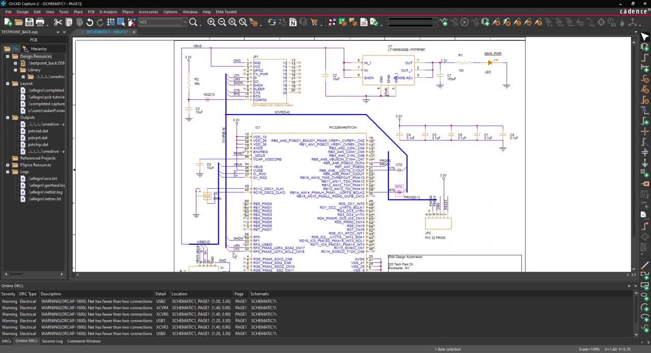
This app allows for automated addition of testpoints to nets in the schematic using a testprep file from PCB Editor. Learn more
Introducing the EMA Academy
We also launched our new EMA Academy portal in Q1. This is our new space to house and share all our learning materials, so they are easily accessible.
New Courses:
We added new ones in Q1 as well (As part of Support+ customers have access to all our free courses as well as discounted access to paid courses):
- Advanced PCB Editor Training Bundle
The Advanced PCB Training Bundle will teach you how to use the advanced features of OrCAD PCB Editor Professional to complete cutting-edge PCBs accurately and efficiently and includes the following modules (which can be taken separately)- Advanced PCB Editor Training for DFM
Learn how to minimize issues during the manufacturing, assembly, and testing of your PCBs with the Advanced PCB Editor Training for DFM. - Advanced PCB Editor Training for Constraints
Learn how to implement rules & ensure success for rigid-flex, differential pairs, and more with the Advanced PCB Editor Training for Constraints. - Advanced PCB Editor Training for Rigid-Flex
Learn how to complete Rigid-Flex PCB’s accurately and efficiently with the Advanced PCB Editor Training for Rigid-Flex Designs.
- Advanced PCB Editor Training for DFM
- DDR SI Metrics Check Workshop
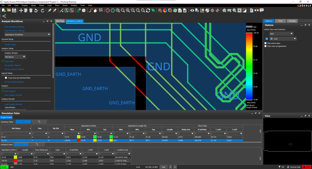
This workshop will teach you how to use the SI Metrics Check workflow in Sigrity to analyze DDR interfaces for crosstalk and reflections.
You can view all our courses here
New How-Tos
Take advantage of our quick step-by-step tips showing how to get the most from your design software. We have over 50 how-tos, with new ones being added weekly based on your feedback. Here are the 20 we added in Q1:
- How to use the OrCAD Capture Free Viewer
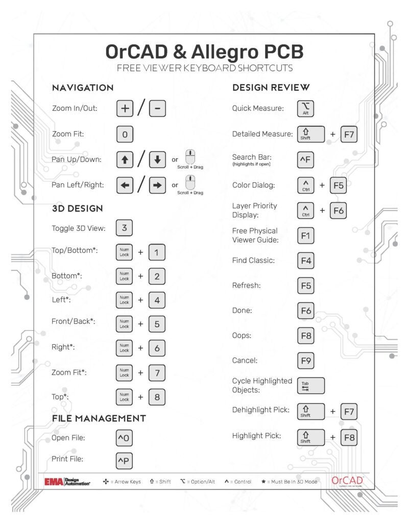
Learn how to use the OrCAD Capture Free Viewer to efficiently and intelligently review schematic designs without tying up a license. - How to use the OrCAD/Allegro PCB Free Viewer
This how-to will teach you how to use the OrCAD/Allegro PCB Free Viewer to intelligently and efficiently review PCB designs. - How to incorporate pin delay and z-axis delay into PCB Design
Learn how to incorporate pin delay and z-axis delay into the PCB design to guarantee accurate length matching for high-speed nets in OrCAD. - How to Check Z-Axis Clearance for your PCB Designs
This quick how-to provides instructions on using Z-DRC in Allegro Productivity Toolbox to check Z-Axis clearances in the PCB Design. - How to Process a PCB for Manufacturing
Learn how to automatically generate a manufacturing output from a centralized location with Post Processing in OrCAD Productivity Toolbox. - How to Compare PCB Designs
Learn how to compare PCB designs and find differences between revisions with PCB Design Compare in OrCAD Productivity Toolbox. - How to Quickly Find Padstacks in a PCB Design
This quick how-to provides instructions on how to find padstacks in the PCB design with Padstack Finder in OrCAD Productivity Toolbox. - How to Generate Oversized Masks for Manufacturing
This quick how-to provides instructions on how to use the Mask Generator in Allegro Productivity Toolbox to create oversized masks while preserving the original padstacks. - How to Generate Test Points in the Schematic After PCB Layout
This quick how-to will provide step-by-step instructions on how to use the Test Point Back Annotation App in OrCAD Capture to efficiently add testpoint from the PCB layout to the schematic. - How to Automatically Adjust Component Labels on a PCB
This tutorial will provide step-by-step instructions on how to use the Label Tune feature with OrCAD PCB Designer Professional and Allegro Productivity Toolbox. - How to Place Components on a Polar Grid
This quick tutorial will provide step-by-step instructions on how to place components using a Polar Grid with OrCAD PCB Designer Professional and Allegro Productivity Toolbox - How to adjust OrCAD for High Resolution Displays
This quick tutorial will provide step-by-step instructions for quickly adjusting how OrCAD displays on high resolution (4k) monitors using environmental variables in windows. - How to Efficiently place components by connectivity
This quick tutorial will provide step-by-step instructions on how to automatically place components based on schematic connectivity with the PCB Clustering App. - How to estimate the board space required for components in your design
This quick how-to will provide step-by-step instructions on how to determine the space required for components on the PCB during the schematic design with the CircuitFit App. - How to reuse IP and Replicate Component Placement
This quick tutorial will provide step-by-step instructions on how to use templates in the PCB Clustering app to replicate component placement for similar circuitry. - How to Perform Noise Analysis
This quick tutorial will provide step-by-step instructions on how to perform noise analysis in PSpice, report the top contributors to noise, and modify the number of top contributors reported. - How to edit net aliases in Bulk
This quick tutorial will provide step-by-step instructions on how to modify net aliases in bulk using OrCAD Capture and Excel to efficiently update net names. - How to Generate Via Shielding in OrCAD
This quick tutorial will provide step-by-step instructions on how to efficiently generate via shielding for the entire board and specific circuitry using the Shield Generator in Allegro Productivity Toolbox. - How to setup Xnets for your PCB Designs
This quick tutorial will provide step-by-step instructions on how to setup XNets for your PCB design using OrCAD Capture and OrCAD PCB Designer. - How to Automatically Create Fillets in OrCAD
This quick tutorial will provide step-by-step instructions on how to automatically create fillets or teardrops on traces with OrCAD PCB Designer. - How to Highlight Parts by Property in the Schematic
This quick how-to will provide step-by-step instructions on how to color-code components on the schematic canvas based on a specific property with the Highlight by Property App.
View all the How-Tos
More to Come
This is just the start. We have lots on our plate in the coming months to keep these updates rolling. With everything we do, we want your feedback. Please let us know your thoughts on these updates and the program in general (feedback form). Most of these initial updates have come from customer questions and requests.
If you don’t think you have access to Support+ yet (it’s free to all active maintenance customers) you can learn more and request access here: EMA Support+
Thanks!


