Bringing a new electronic circuit board to the market is complex and includes several processes and
stages. Depending upon the complexity of the design, development can take weeks or months. Even longer, if you encounter supply chain issues, such as delayed component shipments, manufacturing shortfalls, or obsolescence. Additionally, manufacturing issues can extend the development cycle. Several factors contribute to these major sources of waste. However, with effective electronic product design cost management, you can overcome these challenges and maximize your development ROI.
.
Factors That Drive PCBA Development ROI
PCBA development consists of three distinct but interdependent stages. The fact that design, manufacturing, and testing stages are performed by multiple companies only accentuates the importance of individual optimization and integration between stages. Accomplishing this begins with identifying the important cost factors for development.
|
PCBA DEVELOPMENT COST DRIVING FACTORS |
||
|
Development Stage |
Cost Factor |
Description |
|
Design |
Engineering |
Includes man-hours for circuit design, component selection, and design verification. |
|
Software Tools |
Includes the PCBA design, signal integrity (SI), power integrity (PI), power distribution network (PDN), and thermal and electromagnetic interference (EMI) simulation and analyses. |
|
|
Manufacturing |
Fabrication |
Includes board materials, imaging, etching, hole drilling, and solder masking. |
|
Assembly |
Includes picking and placing parts, soldering components, and inspections. |
|
|
Testing |
Functional Testing |
Includes time domain reflectometry (TDR) and impedance match checking. |
|
In-Circuit Testing (ICT) |
Includes apparatus, such as a flying probe. |
|
|
Structural Testing |
Includes third-party board tests, like HALT/HASS. |
|
As shown in the table above, every stage of PCBA development directly impacts overall cost and ROI. Once a basic design has been created (including component selection, schematic capture, and PCB layout), most development costs can be fixed. It should also be noted that ICT is not typically needed, especially for IPC Class 1 and many Class 2 applications. Further, structural testing, which often involves destructive testing regimens, is only required for critical industries (defense and aerospace) and hazardous environment board implementations.
EDA software costs are often flexible. This is because circuit analysis, RF, and other simulations and analyses for design verification are not included in most PCBA design packages. Therefore, the effectiveness of electronic product design cost management can significantly influence overall PCBA development costs and ROI.
The Importance of Electronic Product Design Cost Management
Effectively managing the costs for designing your board is important for its direct impact and the design process's effect on the cost for all other stages. Excluding special testing regimens, PCBA design has the following impact on development costs.
Impact of PCBA Design on Development Costs
-
→ Design Costs
The costs for designing your board include fixed and variable factors. Your basic EDA program is fixed, but engineering, component selection, and design verification vary according to the project specifications. For example, component availability and other supply chain issues vary greatly from design to design. It is also necessary to ensure that your design meets functional and operational objectives, adheres to industry regulations and standards, and falls within your CM’s DFM and DFA rules and guidelines. These software tool analysis and simulation requirements influence the design and overall development costs. -
→ Fabrication Costs
The PCB fabrication process consists of fixed steps. However, your design decisions can determine exactly how these are performed. For example, the number of layers determines how many substrate-laminate presses are needed. Additionally, your choice of surface mount device (SMD) component packages, number, and type of vias can dictate the type of drill used and how many plated through-holes (PTHs) are required. Other decisions, like solder masks and surface finish types, can also vary in cost. -
→ Assembly Costs
PCB assembly is similar to fabrication because the steps are generally fixed. The exception is for the soldering technique, which is based on types of components. Wave soldering is the most common technique for through-hole parts, which are typically the most costly. However, reflow is used for SMDs. Board cleanings and protection methods such as conformal coating or encapsulation influence costs. -
→ Testing Costs
Manual and optical inspections and some tests, such as automatic optical inspection (AOI), are typically always performed. Other tests, such as TDR, peel (which tests lamination adhesion), Resistivity of Solvent Extract (ROSE), and solder pot and float tests, may not be routine and will often increase the cost.
In addition to these specific stage costs, excessive board respins can also increase development costs. These may be largely unavoidable for some highly complex PCBA designs. However, additional board spins are often required to bring the design specifications in line with the DFM and DFA rules and guidelines for your CM’s equipment or to make changes to improve circuit functionality and operation. Additional costs for performance and manufacturability can be significantly reduced or even eliminated by using PCBA design support software tools.
.
How PCBA Design Support Tools Improve Development ROI
Most PCBA design packages are great for creating schematics and doing PCB layouts. Additionally, most include functionalities to aid engineers and designers, such as constraint management, DRC, auto-routing, and some form of DFM validation. Nevertheless, PCBA design can still be tedious to create a design that meets its operational performance objectives and satisfies your CM’s manufacturability requirements. The additional time, engineering resources necessary, and manufacturing costs can be significant.
Electronic product design and total development costs can be reduced with software development tools. The tools listed below improve the efficiency and accuracy of your design.
Benefits of PCBA Design Support Software Tools
-
★ Supply Chain Integration
Having a component library that includes or incorporates real-time data about availability, turnaround times, and even component life-cycle status can make your part procurement process much more efficient. Having to make component changes downstream can greatly increase development time and costs. -
★ Simulate and Analyze Signal Flows
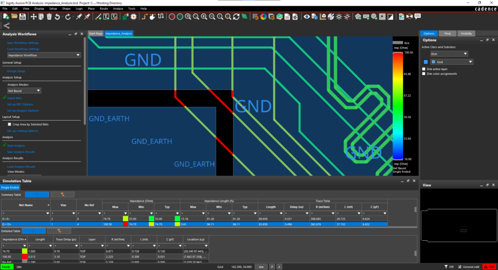
Simulating your circuit’s operation and testing RF and microwave signal flow before the functional testing stage can substantially reduce development time and lower costs for engineering resources and excessive, unnecessary board spins. -
★ Simulate and Analyze Power Distribution
Adequate power distribution is a major concern for many designs. Failure to meet power requirements for your board components, especially ICs, can result in erroneous results. The capability to simulate operation during design ensures your board’s PDN will satisfy on-board and intra-board objectives, saving you from potential board failures and recalls that can be quite expensive. -
★ Simulate and Analyze Thermal Distribution/Dissipation
For high-power components or elements, such as processors and power supplies, the ability to dissipate heat quickly is a mandate that, if unmet, leads to part and board damage. Therefore, this capability can potentially save high unnecessary costs. -
★ More Efficient DFMA Analysis
For most PCBA design packages, DFM verification is a series of back and forth between DFM checks and manual corrections that wastes engineering resources. The alternative of not performing DFM and DFA verification can be increased design⇒build⇒test (DBT) cycles, which is also wasteful. Real-time integrated DFM solves this problem, improving your design process and lowering costs.
Implementing software design support tools that include one or more of the above capabilities will enable you to design faster and more efficiently, lower development costs, and improve your ROI.
EMA Design Automation is a leading provider of the resources that engineers rely on to accelerate innovation. We provide solutions that include PCB design and analysis packages, custom integration software, and engineering expertise, which enable you to create more efficiently. For more information on how to best manage electronic product design cost and ROI and how we can help you or your team innovate faster, contact us.


