 Whether you are new to PCB design or a seasoned professional, the effectiveness of your work depends on an effective process. The design process is driven by unique characteristics, such as your creativity, and evolving heuristics. However, execution efficiency is inextricably tied to the software tools you employ. Today’s complex PCBs require that you employ software tools that exhibit the necessary electronic circuit design essentials for each stage of the process.
Electronic Circuit Design Essentials for Effective Board Development
For all but the simplest of designs, designing circuit boards is an iterative procedure consisting of three distinct yet interdependent phases: design, build and test. Of these, design is the most important as it greatly impacts the efficiency of board build and testing. Design effectiveness depends on the use of software that exhibits the electronic circuit design essentials listed below.| ELECTRONIC CIRCUIT DESIGN ESSENTIALS | ||
| Design Stage | Design Activity | Essential Design Software Attribute |
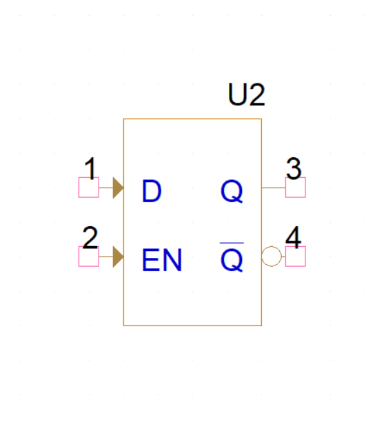
| Schematic Capture | Component Selection | Real-time Component Library |
| Net Creation and Verification | Design Rule Checking (DRC) | |
| PCB Layout | Component Placement | Accurate CAD footprints |
| Trace Routing | Manual and Autorouting | |
| Design Verification | Verify Performance | SI and PI Simulation and Analyses |
| Verify Manufacturability | DFM and DFA Checking | |
Schematic Capture Essentials
A well-developed PCB schematic design checklist provides the best guidance for the initial stage of board design. Schematic design begins with a comprehensive component CAD library, which is your resource for part data and information. For the most effective design and development, your library must include accurate schematic symbols, footprints and 3D models, as well as provide real-time supply chain information. Another essential function performed during schematic capture is net creation and connectivity verification. This task is typically performed by a dedicated design rule checker (DRC). However, leading EDA tools incorporate an integrated rules-based constraint editor and checker that not only identifies netlist violations but also PCB layout errors.PCB Layout Essentials
Laying out your circuit board is the most difficult and time-consuming aspect of the entire design process. However, PCB layout is completely dependent on the actions taken during schematic design. And the layout is also reliant on CAD library data to accurately represent component footprints, landing patterns and reference indicators. Electronic circuit design essentials for your PCB layout software include the soldermask layer data mentioned above, as well as functionality to aid you in placing components and routing traces. There are several options for trace routing; however, the most efficient capabilities include some level of automatic routing with manual adjustment flexibility.Design Verification Essentials
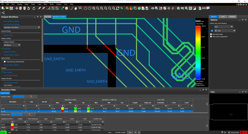
Although not considered one of the two tiers of PCB design, design verification is nevertheless necessary for the most efficient PCB design and development. Traditionally regulated to a post manufacturing experimental activity, verification can be performed during design due to the advancement in product development software. Capabilities; such as checking clearances and spacing for standards and other DFMA rules to ensure manufacturability, help you reduce board spins, minimize turnaround time and achieve reliability, while avoiding wasteful and unnecessary costs. Additionally, incorporating simulation software with capabilities like signal and power integrity (SI/PI) analyses, help minimize functional testing requirements and ensure your board will reliably meet its operational objectives when deployed.Ensuring Design Essentials Implementation
The competitive landscape of the electronics industry demands that you strive to optimize your PCBA development process, as well as ensure the operation and reliability of your boards throughout their projected lifecycle. Meeting this mandate begins with maximizing the effectiveness of your design, which is achievable by following guidelines as below for fully leveraging ECAD software tool capabilities in your design process.
How to Best Incorporate Electronic Circuit Design Essentials
Selecting and incorporating the best electronic circuit design software with the essential capabilities to address your process requirements can be challenging. The best option is probably to partner with an industry leader experienced in helping engineers incorporate software to elevate their design process.
- Be aware of the best ECAD software tools available
- Evaluate your design process and identify areas for improved efficiency
- Select software with needed essential capabilities that will integrate with your EDA tool(s)
EMA Design Automation is a leading provider of the resources that engineers rely on to accelerate innovation. We provide solutions that include PCB design and analysis packages, custom integration software, engineering expertise, and a comprehensive academy of learning and training materials, which enable you to create more efficiently. For more information on electronic circuit design essentials and how we can help you or your team innovate faster, contact us.