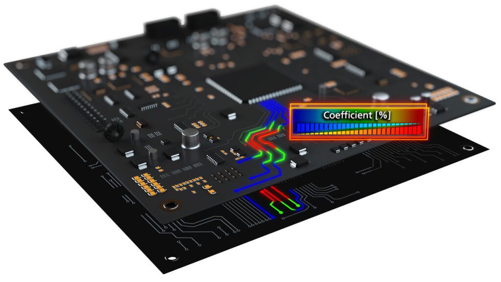
To ensure electromagnetic compatibility (EMC), PCB designers must address issues such as signal and power integrity and radiated emissions to prevent unintended interactions between components and external sources of electromagnetic interference (EMI). This involves careful layout of traces, proper grounding and shielding, selection of appropriate components, and adherence to EMC creepage and clearance standards and guidelines.
Effective PCB EMC design guidelines minimize the risk of malfunction, reduce the need for costly redesigns, and ensure compliance with regulatory requirements, thereby providing reliable and safe operation of electronic devices.
PCB EMC Design Guidelines By Category
The table below provides a comprehensive overview of key PCB EMC design guidelines organized according to design category. These include layout strategies and simulation techniques to ensure optimal performance and compliance with standards.
Design Tools Help Engineers Follow PCB EMC Design Guidelines
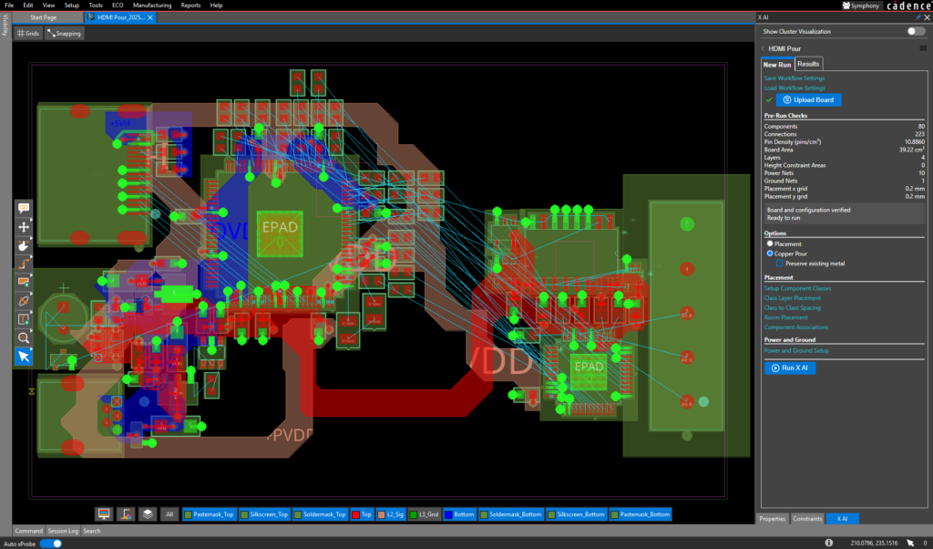
For effective PCB EMC design, you need software with essential functionality and capabilities that optimize PCB design and layout, while enabling EMI minimization. Key features are shown below.
- Electromagnetic simulation tools that allow designers to model and analyze electromagnetic fields, enabling the identification and mitigation of EMI issues before the physical prototyping stage.
- Signal integrity analysis tools that help assess and improve the quality of high-speed signals, reducing noise and reflections that can contribute to EMI.
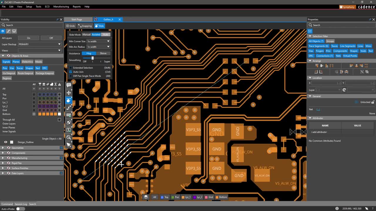
- Controlled impedance routing ensures that traces are designed to maintain consistent impedance. This minimizes signal reflections and noise, which are significant sources of EMI.
- Differential pair routing precision, which helps cancel EMI and reduce radiated emissions.
- Return path management design of low-impedance return paths to reduce loop areas and associated EMI.
- Multilayer stackup design for better shielding and isolation, reducing EMI.
- Ground plane optimization including continuous and well-connected ground planes, which act as effective shields against EMI and provide low-impedance paths for return currents.
- Strategic component placement for optimally placing components to minimize interference between high-speed and sensitive analog components, reducing the risk of EMI.
- Automated routing features that follow best practices for EMI reduction, such as maintaining adequate spacing between high-speed traces and ensuring proper shielding.
- Design rule checks targeting EMI concerns, ensuring the PCB design adheres to EMI reduction guidelines.
- EMI analysis and validation that helps designers to identify potential EMI issues and make necessary adjustments early in the design process.
The best solution to ensure your design is EMC optimized is to partner with an industry expert that will assist you in acquiring and quickly implementing an advanced software tool for implementing effective PCB EMC design guidelines.
EMA Design Automation is a leading provider of the resources engineers rely on to accelerate innovation. We provide PCB design and analysis packages, custom integration software, engineering expertise, and a comprehensive academy of learning and training materials. For more information on effective PCB EMC design guidelines and how we can help you or your team innovate faster, contact us.