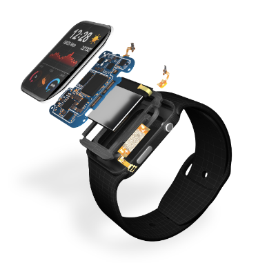
Manufacturing analysis in the context of PCB design involves evaluating the design to ensure it can be manufactured smoothly and cost-effectively without compromising quality. Design for manufacturing analysis must follow DFM guidelines and include thermal integration and yield analyses.
Key practices for design for manufacturing analysis include verifying trace widths, component placement, and electrical connections to prevent defects and reduce costs. By minimizing design complexity and anticipating manufacturing constraints, design for manufacturing (DFM) techniques ensure a streamlined production process, enhancing product quality and reducing time-to-market. Below, we’ve summarized the key PCB design for manufacturing analysis guidelines.
PCB Design for Manufacturing Analysis Guidelines
| Guideline | Description |
| Avoid Floating Copper/Solder Mask Slivers | Prevent noise and interference by maintaining copper features around 4 mils to avoid slivers forming unwanted antennas. |
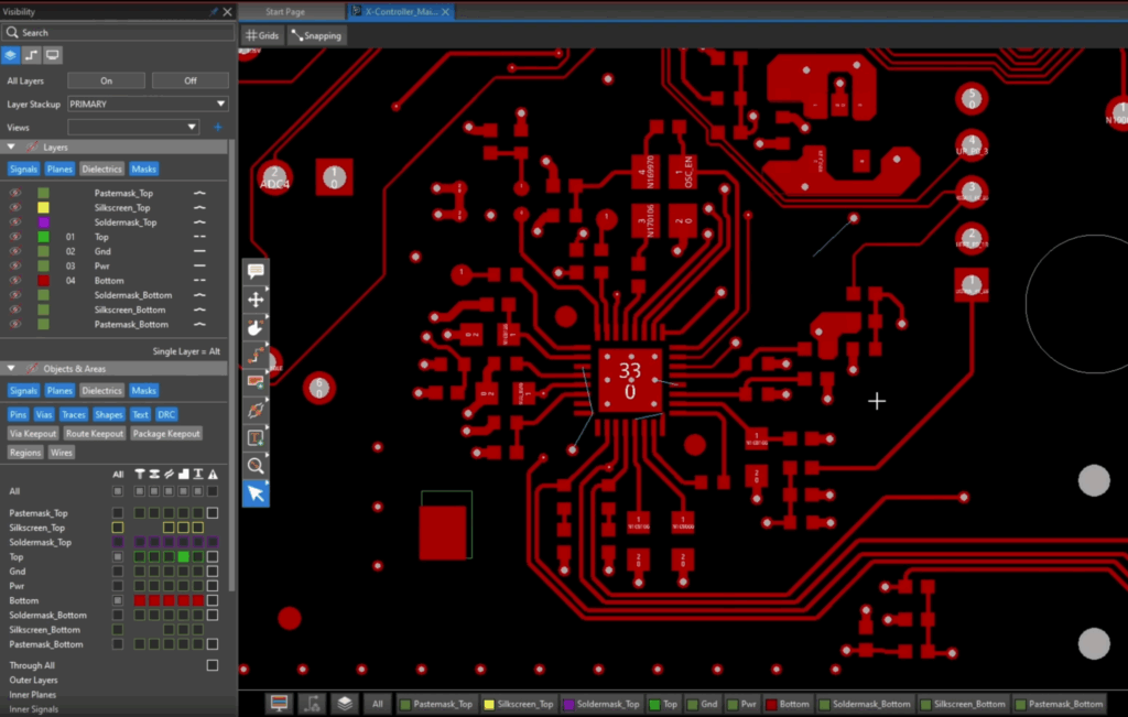
| Keep Design Rules Consistent | Ensure design rules align with manufacturer capabilities using the Design Rule Check (DRC) feature in design software. |
| Keep Copper Away From Board Edges | Prevent shorts in adjacent layers by maintaining sufficient clearance between copper and the board edge. |
| Optimize Trace Widths and Spacing | Use wider traces for higher currents and maintain sufficient spacing to prevent shorts and signal integrity issues. |
| Ensure Sufficient Annular Rings | Ensure annular rings are large enough to accommodate drill misalignment and maintain good electrical connections. |
| Ensure Clearance Pads on Pins | Prevent shorts by ensuring all pins have clearance pads to avoid unintended connections to plane layers. |
| Understand Manufacturer Capabilities | Familiarize yourself with the manufacturer’s capabilities and limitations, such as minimum trace widths and drill sizes. |
| Minimize Layer Count | Reduce the number of layers to lower manufacturing complexity and cost, while maintaining signal integrity and power distribution. |
| Component Placement and Orientation | Place components with similar functions together, align components for easier assembly, and provide enough space for soldering and rework. |
| Avoid Starved Thermals | Ensure thermals have sufficient connections to prevent soldering issues and ensure robust joints. |
| Maintain Proper Annular Ring Clearance | Avoid open circuits by specifying drill sizes that do not exceed the annular ring size. |
| Design for Thermal Management | Implement thermal vias, heat sinks, and copper pours to manage heat dissipation effectively. |
For more information, check out our 10 Common DFM Issues and How to Solve Them eBook.
Thermal Integrity and Yield Analysis Prepare Designs for Manufacturing
Thermal integrity analysis and yield analysis are two crucial methods that aid in optimizing PCB design for manufacturing.
- Thermal integrity analysis involves evaluating a PCB’s ability to manage and dissipate heat during operation.
- Yield analysis as part of PCB Design for Manufacturing (DFM) focuses on maximizing the number of defect-free boards produced during the manufacturing process. This involves identifying and mitigating factors that can cause defects, thereby improving overall production efficiency and reducing costs.
Thermal Integrity Analysis Aspects That Support Design for Manufacturing
| Aspect | Description |
| Heat Generation and Dissipation | Evaluating heat produced by components and ensuring effective dissipation through PCB materials. |
| Thermal Conductivity of Materials | Assessing thermal conductivity of PCB substrates like FR4, polyimide, or metal-core materials. |
| Thermal Management Components | Utilizing heat sinks, thermal vias, thermal pads, and conductive adhesives to enhance heat transfer as needed. |
| PCB Layer Stack-Up | Designing the PCB layer stack-up to improve thermal performance with thicker copper layers or heat-spreading layers. |
| Temperature Gradients and Hot Spots | Identifying and mitigating areas with significant temperature differences to avoid thermal stress. |
| Thermal Simulation | Using software tools like FEA to simulate thermal conditions and predict temperature distribution. |
| Thermal Testing and Validation | Conducting physical tests with thermocouples, infrared cameras, and thermal imaging to validate designs. |
| Cooling Solutions | Implementing active or passive cooling solutions such as fans, heat pipes, or liquid cooling systems. |
| Design Guidelines and Standards | Adhering to industry standards like IPC-2221 and IPC-2152 for thermal management in PCB design. |
Yield Analysis Aspects That Aid in Manufacturing Reliability
| Aspect | Description |
| Design Rule Checks (DRC) | Ensuring the PCB design adheres to manufacturer specifications and detecting potential design errors. |
| Material Quality | Using high-quality materials and ensuring consistency to reduce defects like delamination or conductor issues. |
| Layer Alignment | Ensuring precise alignment of layers during lamination and using optical inspection to verify alignment. |
| Via Integrity | Ensuring proper drilling and plating of vias to avoid voids and withstand thermal/mechanical stress. |
| Solder Mask and Silkscreen | Applying solder masks and silkscreens accurately and ensuring proper curing and adhesion. |
| Component Placement and Soldering | Ensuring accurate placement of components and optimizing reflow soldering profiles to prevent defects. |
| Testing and Inspection | Implementing ICT, AOI, and X-ray inspection to detect defects and ensure proper functionality. |
| Process Control and Monitoring | Using SPC to monitor manufacturing processes and implementing continuous improvement based on yield data. |
| Prototyping and Pilot Runs | Conducting prototyping and pilot runs to identify potential yield issues and make iterative improvements. |
In order to perform effective PCB design for manufacturing analysis, it is essential to follow robust DFM guidelines along with thorough yield and thermal integrity analyses. For the best results, it is necessary to employ leading PCB design support software tools to optimize cost-effectiveness and product quality.
EMA Design Automation is a leading provider of the resources engineers rely on to accelerate innovation. We provide PCB design and analysis packages, custom integration software, engineering expertise, and a comprehensive academy of learning and training materials. For more information on effective PCB design for manufacturing analysis and how we can help you or your team innovate faster, contact us.