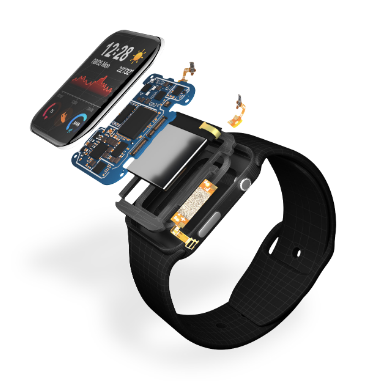
Users want their electronic devices to have their cake and eat it, too, regarding performance and power consumption. Better performance means quicker execution, more robust applications, multithreading, and other operation requirements that align with user demands. Of course, realizing this improved performance comes at the cost of greater power consumption, increasing the rate of energy consumption that increases costs or depletes stored charge. Clever topology and material research have greatly decreased the digital circuit power consumption rate, and designers can utilize some fundamental layout tips to maximize the power-performance trade-off.
The Components of Digital Circuit Power Consumption
Power consumption is an ever-present issue, especially as the domain of portable devices grows in sophistication – users want performance and efficiency, which are naturally at odds. Mitigating energy efficiency losses is one of the keys to optimizing board performance and controlling product design and development costs. We can group power consumption into two general factors:
- Static power, i.e., P = IV, where the current represents quiescent operation and leakage (gate, junction, etc.)
- Dynamic power (P = ACV2f)
- A is the activity factor or the fraction of the digital nodes switching states from low to high. Selectively gating these nodes can lower the dynamic power draw, but many nodes switching states simultaneously can also lead to a current spike.
- C is the internal parasitic capacitance between gates and the switching capacitance during state switching, where both transistor types conduct simultaneously. Smaller transistors and deliberate IC floorplanning can minimize this effect.
- V is the source voltage; increasing or decreasing the value has a quadratic effect on the dynamic power calculation.
- f is the clock frequency. Updating the system state less frequently decreases power consumption (and vice versa).
Thus, total power consumption or power budget is the sum of the static and dynamic contributions. There are power consumption optimization techniques that are out of the hands of the board layout designer. For example, software solutions like dynamic voltage control and frequency scaling are operational factors that can improve power management once the board is implemented or post-hardware design. With that said, an optimized layout does provide the best foundation for optimal performance.
Heat generation is also essential to power consumption: electromagnetic energy is not conservative when working with non-ideal materials, so a portion of the energy stored or transmitted transforms into heat energy. Even those without engineering backgrounds are familiar with this relationship when running a taxing application on their smartphone or computer. What’s more critical to understand is what happens after the local device temperature rises: an increase in temperature opposes electron flow due to the effects of thermal resistance, meaning that system execution suffers. This change may be negligible at small temperature increases due to active and passive cooling features. Depending on the design requirements, this will either necessitate a decrease in performance or efficiency; for example, as a battery experiences greater ambient temperatures, it incurs greater losses that increase the depletion rate.
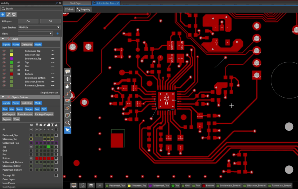
Addressing Power Consumption During Board Layout
Layout designers are responsible for the power distribution network, or PDN, that distributes the necessary net voltages and current requirements throughout the board. Bypass capacitors are critical to providing consistent power: bypass capacitors act as local charge reservoirs when power drawn elsewhere in the circuit threatens to undermine the nearby minimum power demands. Nearly every IC will have at least one, and likely many, bypass capacitors of different nets and sizes to ensure continuous operation.
Designers will want to place the smallest capacitors closest to the same-net IC power pins; if the placement does not inhibit the pin fanout, a direct connection to the capacitor with a parallel via termination (or via-in-pad) is best. Larger bypass capacitor placement should increase radially away from the power pins in question, as the design will want the lowest impedance and loss for the fast charging/discharging bypass capacitors closest to the power pins. Employing bypass capacitor optimization techniques can greatly contribute to lowering digital circuit power consumption.
Clock fanout also maintains a synchronous system’s power consumption and signal integrity. While all signals need routing that prevents EMI issues, the critical signals of a design require additional forethought; these are often the signals that designers must route before any others to preserve minimum trace lengths/via transitions for low-impedance. Given the importance and preponderance of the digital clock line pins/routes across a synchronized circuit, designers want to avoid running traces close to high di/dt lines (think inductors on a switched-mode power supply) that can induce a current on nearby traces. The coupling of the signal can either interact constructively (parallel to signal propagation) or destructively (antiparallel); the former can increase dynamic power drawn and potentially damage sensitive circuits running near maximum ratings, while the latter can disrupt timing across the circuit and lead to runtime errors that are difficult to diagnose.
EMA Offers Powerful Design Solutions
Well-optimized digital circuit power consumption ensures long device uptimes without needing improvements in battery technology or general savings in energy usage/thermal management for non-portables. Power consumption is a major concern, as it informs operational efficiency and design concerns, like thermal distribution and dissipation. Product design and development tools; including Celsius EC and Sigrity, that simulate system-level thermal design and signal integrity, can be implemented to create the most advantageous power budget for your design. EMA offers these products and other ECAD tools to ensure optimal performance in your electronic PCBAs and systems built from the ground up.
EMA Design Automation is a leading provider of the resources that engineers rely on to accelerate innovation. We provide solutions that include PCB design and analysis packages, custom integration software, engineering expertise, and a comprehensive academy of learning and training materials, which enable you to create more efficiently. For more information on digital circuit power consumption and how we can help you or your team innovate faster, contact us.