Double Data Rate 5 (DDR5) is the latest generation of synchronous dynamic random-access memory (SDRAM), succeeding DDR4. DDR5 offers significant improvements in bandwidth, capacity, and power efficiency, making it ideal for high-performance applications such as data centers, gaming, and artificial intelligence.
This technology operates at much higher frequencies than its predecessors, necessitating specific DDR5 signal integrity considerations. Read on as we discuss how to ensure DDR5 signal integrity.
PCB Layout Guidelines for DDR5 Signal Integrity Essentials
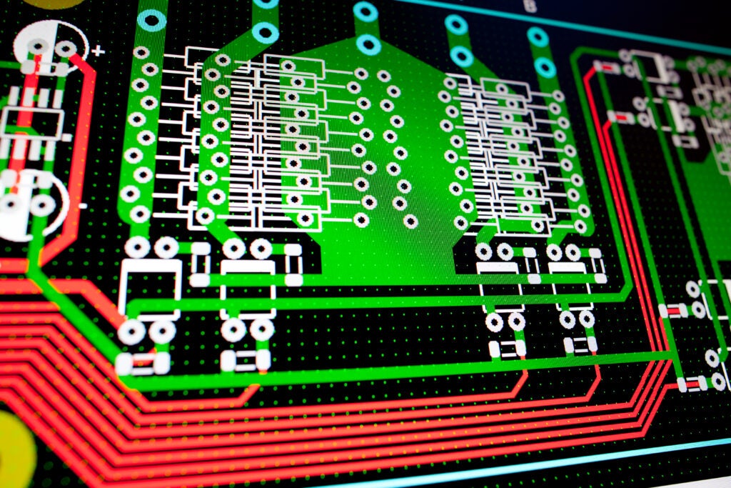
DDR5’s higher speeds and lower supply voltages introduce strict margins and tolerances in PCB layout and design. Here are essential guidelines to ensure signal integrity:
PCB LAYOUT DESIGN GUIDELINES FOR DDR5 SIGNAL INTEGRITY | |
Category | Guidelines |
Impedance Control | – Maintain consistent trace impedance – Use controlled impedance traces (e.g., 50 Ω) – Avoid impedance discontinuities |
Trace Routing Guidelines | – Keep traces as short as possible – Match trace lengths – Follow specified spacing rules for DDR5 signals (generally 3 times the trace width (3W) between parallel signal traces). |
Termination Techniques | – Implement proper termination resistors – Use series or parallel termination as needed – Integrate on-die termination (ODT) and on-module power management ICs (PMICs) as necessary |
| Differential Signaling | – Route differential pairs together – Match trace lengths and impedances – Maintain constant spacing between differential pairs |
Signal Return Paths | – Ensure continuous ground planes – Avoid split planes under high-speed signals – Provide low-inductance return paths |
Jitter and Timing Analysis | – Analyze timing margins – Account for jitter in clock and data signals – Use timing analysis tools for validation |
| Eye Diagram Analysis | – Check for eye opening and closure issues – Identify sources of signal degradation |
| Signal Loss and Attenuation | – Use appropriate trace widths and materials – Account for skin effect at high frequencies – Use ultra-low-loss dielectric materials specifically optimized for DDR5 frequencies. |
Noise Margins and Thresholds | – Ensure sufficient noise margins – Validate signals against voltage thresholds |
Grounding Strategies | – Use solid ground planes – Avoid ground loops – Connect grounds appropriately between PCB layers |
Signal Timing and Skew Management for DDR5 Signal Integrity
Accurate signal timing is crucial for DDR5 signal integrity. Managing signal skew involves ensuring that all signal traces have matched lengths to synchronize signal arrival times. Key strategies include:
- Length Matching: Ensure all signal traces are length-matched to synchronize signal arrival times.
- Buffering and Equalization: Utilize signal buffers and equalization techniques to compensate for signal degradation over long trace lengths.
- Effective skew management ensures that data is accurately captured, reducing the likelihood of timing-related errors and enhancing overall system performance.
Decision Feedback Equalization (DFE)
DFE operates by correcting signal distortions caused by previous bits affecting the current bit (post-cursor ISI). The key idea behind DFE is to use the decisions made on previously detected bits to predict and cancel out their effect on the current bit being detected. This is done in real-time as data is being processed. DFE directly influences both timing and skew by improving the overall quality of the signal, allowing the system to maintain tighter timing margins and manage skew more effectively.
In DFE, a Feed-Forward Equalization (FFE) tries to counteract pre-cursor Inter-Symbol Interference (ISI)—interference caused by future bits. It adjusts the incoming signal using a filter that compensates for this type of distortion. It operates linearly, meaning it applies fixed weights (coefficients) to the incoming signal based on how much interference is expected from nearby bits.
Post-Cursor ISI
DFE tackles post-cursor ISI—interference from previously received bits by looking at the decisions already made about earlier bits and using those decisions to predict and cancel out their interference on the current bit. DFE takes the previously detected bits and feeds them back into the equalizer. These bits are multiplied by pre-calculated coefficients that model how much ISI each previous bit introduces to the current bit.
- The ISI contributions from these previous bits are then subtracted from the current bit, effectively “cleaning up” the signal and making it easier to correctly detect whether the current bit is a 1 or 0.
DFE Decision Process:
- The incoming signal is received, and the first part of the equalizer (FFE) filters out pre-cursor ISI.
- The equalized signal is sent to the decision block, which determines whether the current bit is a 1 or 0.
- The decision on the current bit is fed back into the DFE, which uses it to subtract any ISI it might introduce to the following bit.
- This feedback loop continues, ensuring that post-cursor ISI is constantly being compensated for as new bits are received.
Eye Diagrams to Determine Signal Integrity
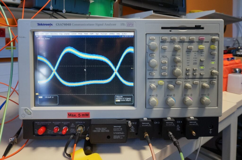
The eye diagram, which can be obtained from DDR5 simulation, is an important indicator for assessing the signal integrity of a channel. It is generated by passing pseudo-random binary sequences (PRBS) through the channel. In the case of DDR5’s write cycle, the controller (acting as the transmitter) sends PRBS to the memory module (the receiver), which constructs the eye diagram by layering segments of these PRBS patterns.
Signal integrity is judged by comparing the eye diagram with an eye mask, which visually represents the receiver’s threshold. A wide-open eye suggests that the signal integrity is strong, allowing the receiver to accurately differentiate between ones and zeros. In contrast, a closed eye suggests overlapping signals, increasing the risk of bit errors.
Impulse Responses in DDR5
The impulse response measures how a channel transmits a single bit with a specific edge rate through the channel. It depicts how an instantaneous electrical pulse travels through the DDR5 channel, revealing the influence of channel properties like attenuation, reflection, and dispersion. By examining the impulse response, engineers can detect distortions such as inter-symbol interference (ISI) and crosstalk that occur at high data rates. This examination allows for the development of equalization and filtering techniques to reduce these distortions, ensuring better DDR5 signal integrity.
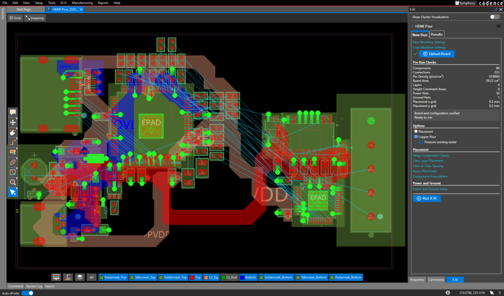
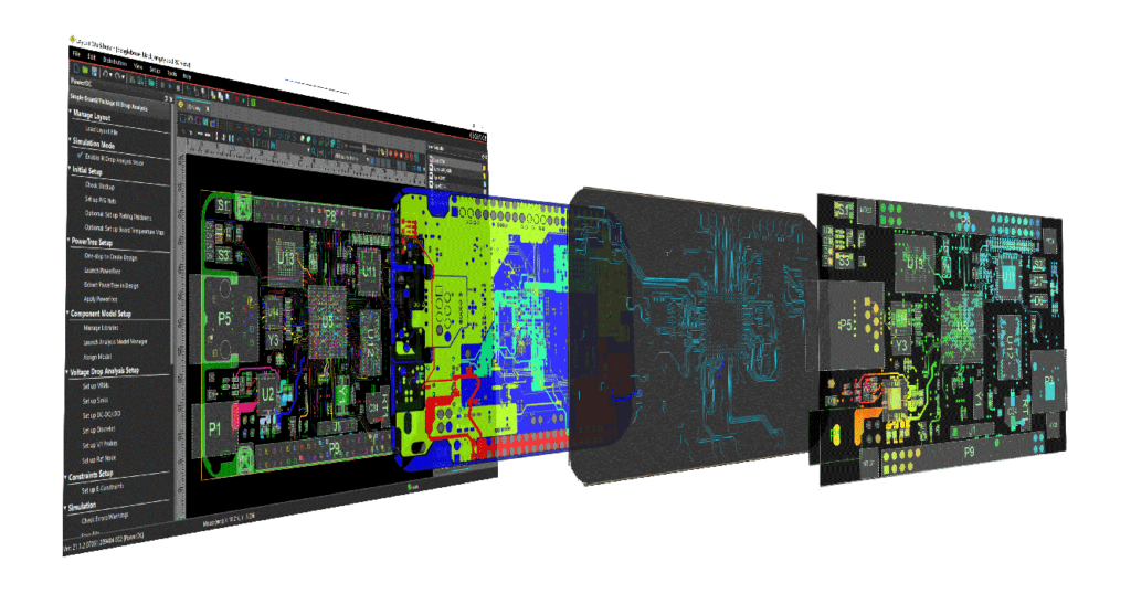
Using electronic design automation (EDA) software for ensuring DDR5 signal integrity through prototyping and post-layout crosstalk simulations can help evaluate and optimize designs. These tools assist in analyzing reflections and ensuring impedance matching. Use advanced simulation tools to model the high-frequency behavior of PCB traces, vias, connectors, and other interconnects.
For more information on DDR5 simulations and post-layout verification, see these webinars:
- A Dive Into DDR5: An Engineer’s Guide to Simulating and validating the Latest Version of DDR.
- DDR5 Post-Layout Verification: Find and Fix Causes of Failures.
EMA Design Automation is a leading provider of the resources that engineers rely on to accelerate innovation. We provide solutions that include PCB design and analysis packages, custom integration software, engineering expertise, and a comprehensive academy of learning and training materials, which enable you to create more efficiently. For more information on HDI PCB design guidelines and how we can help you or your team innovate faster, contact us.
