Modeling designs help engineers verify whether their circuit will function as intended. Modeling programs simulate circuit behavior under different conditions and in accordance with the design requirements, allowing engineers to better plan and build circuits.
Typically, to model components, generic models are used, which produce inaccurate and unrealistic simulations based on ideal conditions. This can cause functionality issues to go undetected until far later in the design process. To confidently simulate digital designs, create a D flip-flop SPICE model using specifications from a manufacturer’s datasheet.
 Open in New Window
What is a Clocked D Flip-Flop?
Flip-flops are basic elements for storing one bit of information. Flip-flops have their content change only either at the rising or falling edge of the enable signal which is typically the clock signal. After the rising or falling edge of the clock, the flip-flop content remains constant even if the input changes. Flip-flops are more formally known as ‘bistable multivibrator’ because they have two stable states. It can remain in either of the two states indefinitely until directed by any input signal to switch states. A Data flip-flop or D flip-flop is a type of digital storage used in sequential logic circuits.
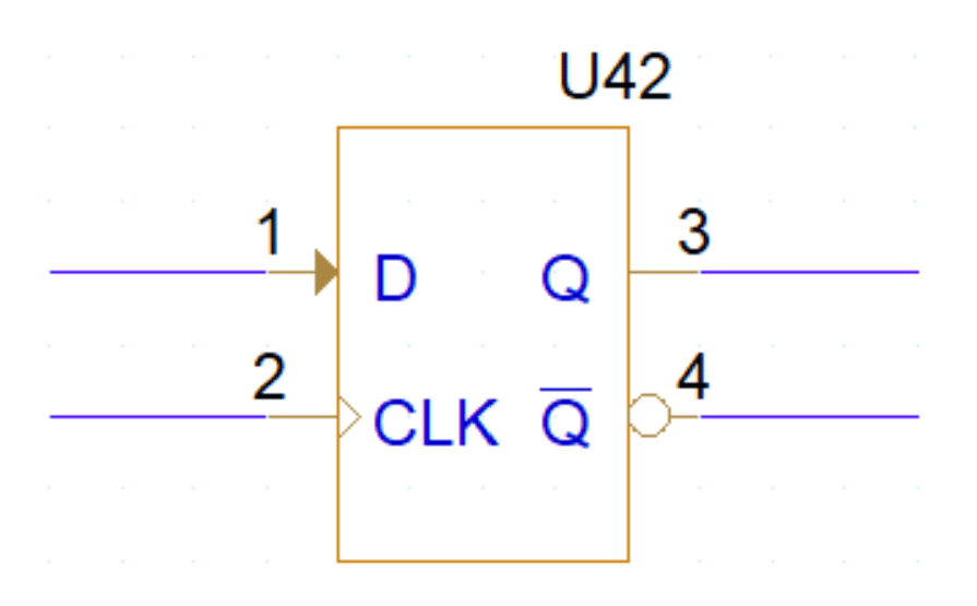
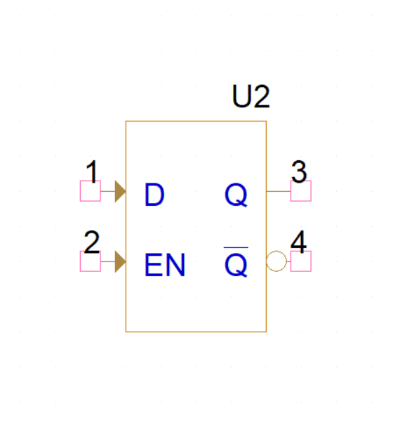
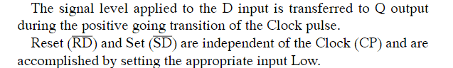
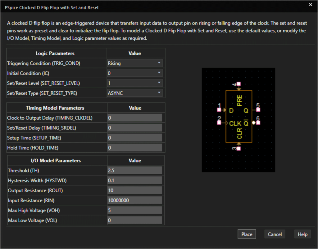
A clocked D flip flop is an edge-triggered device that transfers input data to output pin on rising or falling edge of the clock.
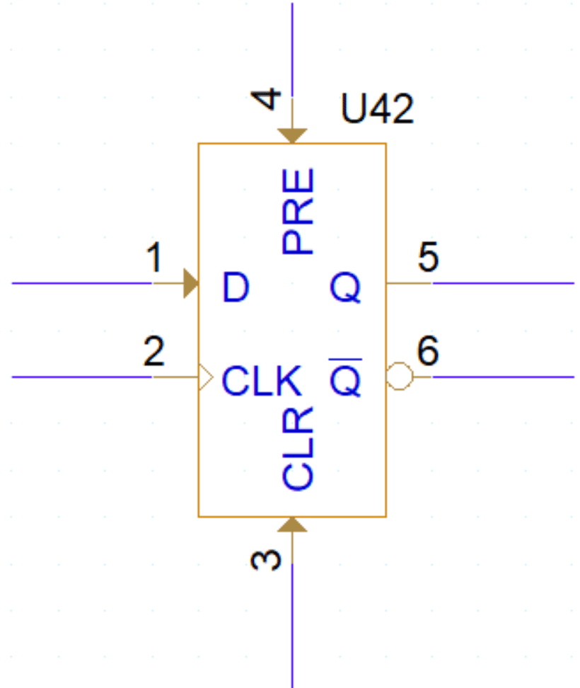
D flip-flops can contain an additional set and reset pin. The set and reset pins work as preset and clear to initialize the flip-flop.
The D Flip-Flop contains the following inputs and outputs:
- Data Input (D): The primary input where the bit of data is provided.
- Clock Input (CLK): The data is captured on either the rising edge or falling edge of the clock signal.
- Primary Output (Q): Primary output reflecting the stored bit.
- Complementary Output (Q-bar): The inverse of Q.
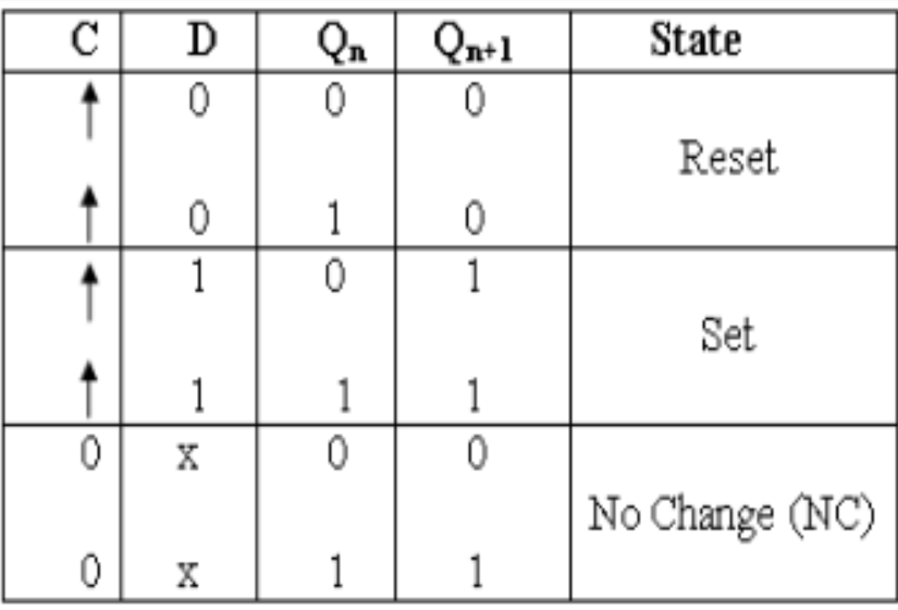
The following truth table below provides detailed operation of a D Flip-Flop:
D Flip-Flops have a variety of applications in digital electronics including:
- Data Storage
- Synchronization
- Shift Registers
- Counters
- State Machines
What is Needed to Model a Clocked D Flip-Flop?
D flip-flops are frequently used in digital applications for sequential logic circuits. In sequential logic circuits the output levels at any instant of time are dependent not only on the levels present at the inputs at that time but also on the state of the circuit. To realistically simulate digital circuit functionality and create a D flip-flop SPICE model for simulation, there are three items that must be defined:
Logic Parameters
For accurate behavioral representation, the triggering condition and initial condition of the D flip-flop must be defined. For D Flip-Flops with set/reset pins, the level (high or low) and type (synchronous or asynchronous) needs to be defined.
Timing Characteristics
Timing is critical to digital design operation and performance. Consider delays as well as setup and hold times for the device.
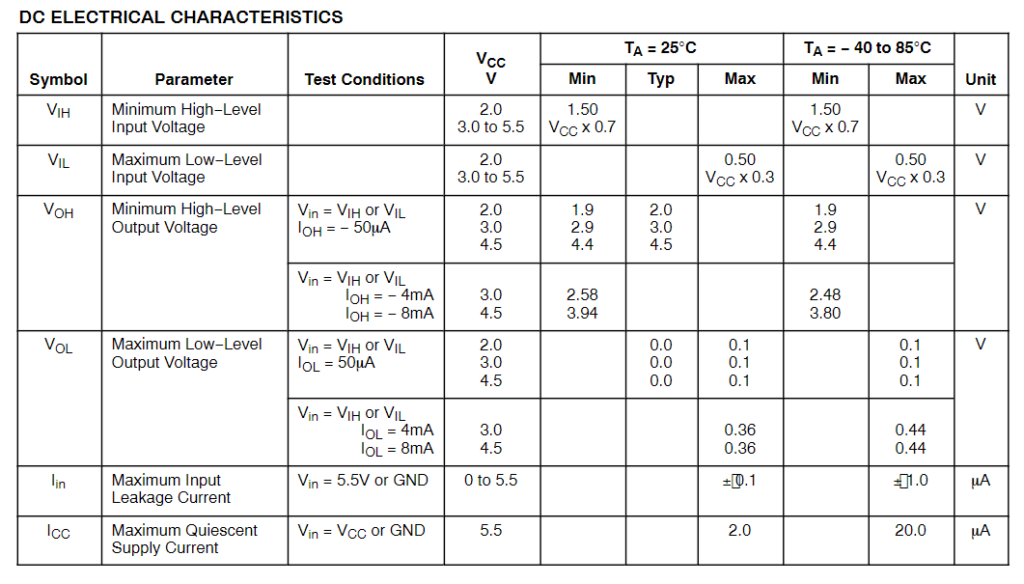
DC Electrical Characteristics
The DC electrical characteristics define the operating conditions for the D flip-flop. This includes:
- The maximum output voltages during high-level and low-level operation
- The voltage levels or thresholds that control the switch from high-level operation to low-level operation
- Hysteresis is often defined for these devices to provide a cushion, ensuring accurate switching between low-level and high-level states even with noisy input signals. It is typically provided by device manufacturers on the device datasheet as VH; however, if not provided it can be calculated by the following equation:
VH = VT+ – VT-
The input is HIGH when it rises above Threshold + (Hysteresis Width/2).
The input is LOW when it falls below Threshold – (Hysteresis Width/2).
Device Resistance
Input and output resistance of the device is critical to the operation and necessary to create an accurate model representation. If this parameter is not provided on the device datasheet, it can be calculated with Ohm’s law.
Input Resistance (RIN)
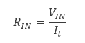
Use the maximum input voltage (VIN) and maximum leakage current (commonly IIN or Il) to calculate the input resistance.
Output Resistance (ROUT)
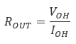
Use the maximum output voltage (VOH or VOL) and the maximum output current (IOH or IOL) to calculate the output resistance.
Once this information is obtained and calculated, these values must be incorporated into the SPICE simulation model which can be achieved by manually creating or editing a text file. Keep in mind if the D flip-flop created does not produce the intended outcome and a decision is made to change components, values will need to be re-calculated and edited manually. This manual process to produce an accurate D flip-flop SPICE model is time consuming and increases the likelihood of errors; however, the PSpice Modeling App provides a fast, easily configurable, and fully integrated method to create buffer or inverter models for simulation.
Creating a D Flip-Flop SPICE Model in PSpice
The D flip-flop modeling application quickly creates D flip-flop SPICE models with a wizard-based approach. To create D flip-flop models, users can easily input the characteristics, defined by manufacturers, directly into predefined parameters:
Triggering Condition
Define the triggering condition as the rising or falling edge of the clock signal. The default condition is set to rising, where a flip-flop toggles the state when the input is high and retains the previous state if the input is low. Positive edge-triggered equates to a rising triggering condition while negative edge-triggered equates to a falling triggering condition.
Initial Condition
Define the initial condition of the flip-flop as 0 or 1.
Set/Reset Level
This parameter is only available when modeling a D flip-flop with set and reset pins. Define the set/reset level of the preset and clear pins as 0 or 1. This is typically defined in the device datasheet.
Set/Reset Type
This parameter is only available when modeling a D flip-flop with set and reset pins. Define the Set/Reset type as asynchronous (ASYNC) or synchronous (SYNC). This is typically defined in the device datasheet.
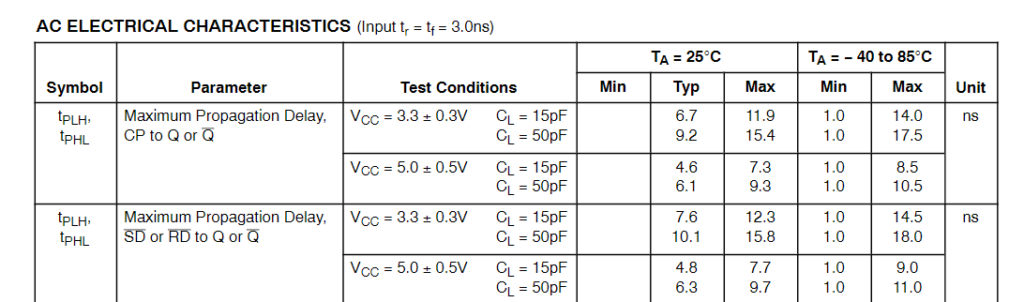
Clock to Output Delay (TIMING_CLKDEL)
Define the time delay between the clock and output pin of the device. The delay is calculated from the triggering edge of the clock to the output in seconds. This is typically defined as tPHL or the propagation delay on device datasheets.
Set/Reset Delay (TIMING_SRDEL)
This parameter is only available when modeling a D flip-flop with set and reset pins. Set or reset the delay of a flip-flop in seconds which is the time between the preset or clear command and the pulse change. This can sometimes be found on the device datasheet as trec or the recovery time.
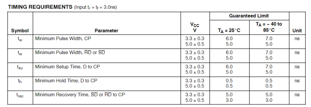
Setup Time (SETUP_TIME)
Define the time duration for which the input remains stable before the arrival of the clock edge (in seconds).
Hold Time (HOLD_TIME)
Define the time duration for which the input remains stable after the clock edge in seconds.
Threshold (TH)
Define the voltage level (V) that indicates a switch between high-level and low-level operation.
Hysteresis Width
Hysteresis is the difference between the positive input threshold voltage and the negative input threshold voltage. It is typically provided on the device datasheet as VH.
Output Resistance (ROUT)
Specify the resistance of the output pin in ohms.
Input Resistance (RIN)
Specify the input resistance at each input pin of the flip flop in ohms.
Max High Voltage
Define the output high voltage. This is typically defined on device datasheets as VOH.
Max Low Voltage
Define the output low voltage. This is typically defined on device datasheets as VOL.
Using the inputted information above, the PSpice Modeling App generates a schematic symbol and automatically associates the newly created D flip-flop SPICE model without leaving the OrCAD Capture environment. The PSpice Modeling App also automatically manages the simulation profile configuration, eliminating any library set up for simulation. Be sure to check out additional SPICE model how-tos and follow along with these step-by-step instructions and download the free trial to try it yourself.