Impedance matching is critical for signal integrity, ensuring maximum power transfer and limiting reflections that degrade signal integrity and potentially damage sensitive components. While components may be the first thing that comes to mind for impedance matching, the transmission line–regardless of type–must also share the characteristic impedance to avoid discontinuities. This controlled impedance design guide will give designers an overview of the implementation process and some step-by-step instructions.
TYPES OF PCB TRANSMISSION LINES | |
Transmission Line | Description |
Embedded microstrip | A trace within the laminated substrate that contains a reference plane on one side and air on the other (i.e., outer layer). |
Offset stripline | A trace within the laminated substrate that contains a reference plane on either side (i.e., inner layer). |
Edge-coupled coated microstrip | The differential analog of the embedded microstrip is parallel in the plane and coated with resist. |
Edge-coupled offset stripline | The differential analog of the offset stripline is parallel in the plane. |
Broadside-coupled stripline | The offset stripline’s differential analog has bases oriented normal to the plane. |
Coated coplanar strips with ground | A single-ended trace surrounded by two planar-parallel ground traces and coated with resist. |
Coated coplanar waveguide with ground | Similar to the above, but with traces widened to be relatively infinite to the signal trace. The ground plane can be on one or both sides of the signal trace. |
Offset coplanar waveguide | The stripline variant of the above. |
Controlled Impedance Design Guide: Traces from the Ground Up
Controlled impedance is a cornerstone of modern PCB stackups, especially in high-speed design. Before any layout work commences, the designer will want to apply circuit analysis techniques to help determine the most effective trace dimensions by layer, as impedance calculations will depend on several factors:
Transmission Line Factors That Impact Controlled Impedance
- The in-plane trace width – width increases, impedance decreases, and vice versa. The bottom width of the trapezoid (formed due to the differing time durations in which the etchant solution contacts the copper layer vertically) is the value communicated between manufacturers and designers to establish yield/cost.
- The vertical trace thickness. Thicker copper foils result in thicker trace thicknesses and increase the minimum trace width. The trace thickness reported is usually the finished value, i.e., post-plating.
- Vertical distance to the nearest reference plane(s). Closer planes increase capacitive coupling but decrease the loop area by bringing the return current’s path closer.
- The gap distance between two differential-coupled traces (if applicable) that run in parallel to cancel EMI.
The dimensions of the traces are only one aspect of a controlled impedance and the larger stackup, as many layers will neither be a conductor nor even contain signal fanout. The dielectric material – both the thickness and dielectric constant – dramatically affects the capabilities of the PCB.
Board Material Impact on Controlled Impedance
The location of the controlled impedance traces will also change the type of transmission line: traces on the outer layers will have different impedance values than those on the inner layers, regardless of whether all the physical dimensions of the trace are identical.
Many controlled impedance lines on a PCB are 50Ω single-ended or 100Ω differentially paired, but specific protocols will diverge from this standard, such as USB, HDMI, video coax, and more. Next, designers should determine the minimum component pitch fanout – this will usually be a high pin-count package like a BGA. From here, two or three trace variables remain. The copper foil/trace thickness will depend first on any additional current-carrying necessary for the design, followed by cost – 1 oz./sq. ft. is the most common pre-plating thickness for this reason. The distance between the planes is also variable according to the thickness needs of the finished board, and this will reflect substrate costs, material on hand, dielectric constant values, and other intrinsic material properties (if in doubt, talk to your manufacturer!)
Unless there are additional design constraints, designers can modify the thickness as they see fit, provided there’s a balanced distribution of core and substrate materials about the board’s vertical center. So, with the trace width and thickness fixed, designers can modify the substrate thickness between conductor layers by adding, removing, or substituting different substrate thicknesses until the overall stackup thickness conforms to the stated design constraint and the impedance structures for every layer are as close as possible to the intended impedance values.
Controlled Impedance Verification
A manufacturer can confirm the impedance values of the bare board by performing time-domain reflectometry (TDR) testing. TDR tests check transmission lines or trace impedances by applying a signal and measuring any reflective signal properties. PCB coupons are a standard practice that utilizes sacrificial pieces of the panel for TDR and other in-depth analyses. Since the coupon originates from the reserved area of the panel, it undergoes the same process conditions as the bare board, and destructive testing doesn’t impact the lot yield. Even if yield were not a concern, the coupon tends to give more accurate measurements of the impedance structures than analysis of the bare board due to the following issues:
- Controlled impedance traces may not be readily accessible; think inner layer traces or closely situated ground planes.
- Testing requires a trace of 150 mm/6” for reliable, repeatable measurements, which is exceedingly rare to encounter on the board as routing density increases and designs shrink.
- Any branched segments or vias complicate the measurement/calculation process.
- Not only is there unlikely to be enough space to include the coupon features on the PCB, but their inclusion naturally affects the performance/characteristics of the design.
Additionally, the designer can assist the manufacturer by leaving clear, unambiguous instructions for impedance testing. Documentation should include the layers containing controlled impedance lines, the impedance values found on that layer (can be one or many depending on the number of distinct characteristic impedance lines, the presence of single-ended and differential pair lines, etc.), and the width of the controlled impedance trace. Providing straightforward and thorough documentation instructions during project packaging will reduce the chance of miscommunication and turnaround time.
For more detailed guidance and steps for controlled impedance design, see this eBook.
Let EMA Guide Your Board Design
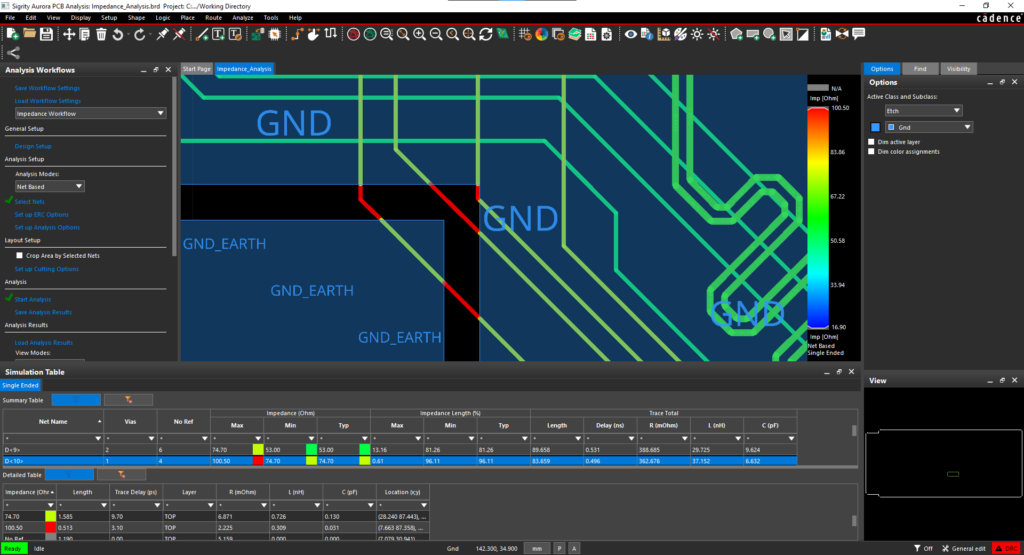
A controlled impedance design guide is an important asset to help create board designs that support development efficiency by ensuring the design conforms to many DFM and DFA requirements while still meeting its performance goals before manufacturing. Employing product design software can be an invaluable asset to achieve your design objectives and maximize ROI. EMA provides leading ECAD software solutions like OrCAD X that help shorten lead times and minimize development costs, with advanced capabilities for defining and managing controlled trace impedance in real-time as you design.
EMA Design Automation is a leading provider of the resources that engineers rely on to accelerate innovation. We provide solutions that include PCB design and analysis packages, custom integration software, engineering expertise, and a comprehensive academy of learning and training materials, which enable you to create more efficiently. For more information on controlled impedance design guides and how we can help you or your team innovate faster, contact us.


