Virtually all engineers and PCB designers today have abandoned the old black box model of circuit board development. The ever-increasing demands for greater functionality and performance, coupled with the competition to meet these mandates, make white box development, which integrates design intent and contract manufacturer (CM) DFM and DFA requirements, imperative. However, making sure your board can be built does not ensure the most efficient PCB development process.
Not only do your boards have to satisfy manufacturing classification standards, but they have to operate reliably and achieve your performance goals once installed. It is not uncommon to rely solely on post manufacturing functionality testing to validate your design. Doing so; however, can lead to redesigns, increased turnaround times, delivery delays, excessive costs and decreased ROI. The best way to avoid these negative contingencies, which is the primary reason for digital twin implementation, is to leverage circuit simulation advantages to improve development efficiency.
The Advantages of Circuit Simulation
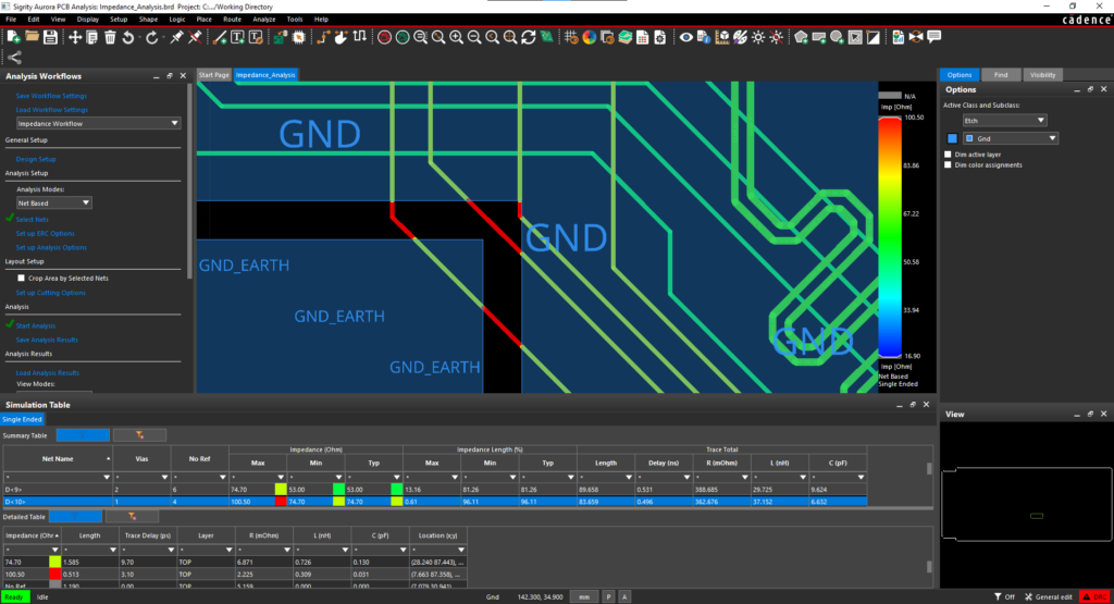
For PCBA development, the use of a software model of a physical circuit board, or a digital twin, is becoming more and more common. The ability to visualize, inspect and analyze a 2D or 3D rendering of the hardware embodiment helps developers and manufacturers reduce the number of design⇒build⇒test (DBT) iterations necessary for prototyping by simulating operation cases and making changes before manufacturing. Although digital twin technology is relatively new, leveraging the advantages of simulation to improve circuit board development efficiency is not.
The top circuit simulations and the advantages of employing them are listed below.
The list above is not exhaustive. In fact, with the right product design and development software you can employ simulation to most aspects of the PCB design process. However, the list above clearly demonstrates how employing circuit simulations can significantly improve PCBA development efficiency.
Optimizing Circuit Simulation Advantages for Your Design
The quality of your PCB design process impacts all aspects of circuit board development. Although design quality is a variable, it can be quantified to a great degree. The most important defining factors are whether or not your PCB design is ready for first-time right manufacturing and whether that fabricated and assembled board achieves the functionality and performance objectives. The first, manufacturability, depends on the incorporation of your CM’s DFM rules and guidelines. The latter, operational reliability, is best assured by optimizing circuit simulation advantages.
Keys to Optimizing Circuit Simulation Advantages
🔑 Know the types of simulation software available and their advantages.
🔑 Identify aspects of your process that can be improved by employing simulation.
🔑 Choose simulation software that integrates with your EDA program and is scalable.
🔑 Ensure your simulation solution is well-supported to minimize any learning curve.
🔑 Partner with an experienced simulation software provider.
Following the keys above is the best path to acquiring and implementing product design software to maximize PCB development efficiency by leveraging circuit simulation advantages.
EMA Design Automation is a leading provider of the resources that engineers rely on to accelerate innovation. We provide solutions that include PCB design and analysis packages, custom integration software, and engineering expertise, which enable you to create more efficiently. For more information on circuit simulation advantages and how we can help you or your team innovate faster, contact us.