When designing printed circuit boards (PCBs), following PCB via and pad size guidelines are critical to ensuring the board’s reliability and performance. This guide will delve into the intricacies of PCB via types, their sizing criteria, and the importance of pad size selection.
PCB VIA TYPES AND IMPORTANT ATTRIBUTES | ||
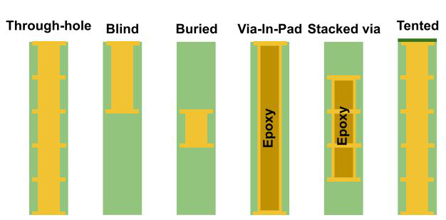
Via Type | Description | Benefit |
Through-hole Via | Extends through the entire thickness of the board. Commonly used for high-current connections or mechanical support. | Provides a continuous connection between all layers. |
Blind Via | Connects an outer layer to one or more inner layers without going through the entire board. | Utilized in high-density designs to save space. |
Buried Via | Connects two or more inner layers without reaching the outer layers. | Ideal for high-density designs needing many inner layer connections. |
Via-in-Pad | Positioned directly under a component pad. Enables direct connections, reducing trace length and improving signal quality. | Minimizes solder bridging risk by being filled with conductive material during assembly. |
Micro Via | Typically, less than 6 mils in diameter. Suits high-density designs where space is limited. | Beneficial in high-frequency applications for maintaining signal integrity. |
Consists of multiple vias stacked on top of each other. | Enhances connection capabilities in dense PCB layouts without increasing board size. | |
Via Tenting | Covers the via with non-conductive materials like solder mask or epoxy. | Protects against contaminants and moisture. Enhances board aesthetics and prevents accidental short circuits. |
Considerations for Choosing PCB Via Size
When choosing a via, first consider its function. Specifically, whether it needs to carry a signal or significant power, it should be large enough to carry enough current to complete the circuit. In this case, consider using a via aspect ratio calculator, which determines the optimal aspect ratio (depth to diameter) for vias —this affects current conduction and plating thickness.
Thermal vias, on the other hand, have the primary role of dissipating heat to prevent damage. Tented vias are generally used to prevent current flow and aid in solder flow — they are typically small (0.25 to 0.3 mm) and may require laser drilling.
PCB Via Size Guidelines
PCB via size guidelines are influenced by several factors, including board classification, fabricator capabilities, and board and via density. Board classification determines the via size based on the component density, which is categorized into three major categories.
- Level A represents low-density designs with via sizes typically around 20 mils (0.5 mm) or larger, used in less complex boards with wider spacing between components.
- Level B corresponds to moderate-density designs with via sizes around 10-20 mils (0.25-0.5 mm), accommodating a balanced number of components with medium spacing.
- Level C denotes high-density designs requiring via sizes smaller than 10 mils (0.25 mm), necessary to fit a large number of components in tight spaces, often seen in advanced and miniaturized electronics.
In general, for standard boards, a common via size is 10 mil, or 7 mil after plating, and microvias as 4 mil.
PCB Pad Size Guidelines
The pad size, also known as the annular ring, is the distance from the finished hole wall to the edge of the pad (external layers) or from the drill hole wall to the edge of the pad (internal layers).
IPC-2221 and IPC-6012 standards provide guidelines on minimum annular ring sizes and fabrication allowances. A good rule of thumb for the minimum pad diameter is L=a+2b+c, where:
- a = Diameter of the finished hole (external) or drill hole (internal)
- b = Minimum annular ring size
- c = Minimum standard fabrication allowance for interconnect lands
Alternatively, you can also use a PCB annular ring calculator to get the optimal size for copper rings around a via.
IPC Standards for Pad Sizes
In addition to hole sizes, pad diameters must be considered based on component density. IPC-2221 provides guidelines for pad diameters:
- Level A requires a pad diameter that is at least 0.5 mm larger than the hole size.
- Level B specifies pad diameters that are 0.3 mm larger than the hole size.
- Level C demands pad diameters that are 0.2 mm larger than the hole size.
It’s important to note that the IPC standards don’t explicitly tell you how to design your PCB or what pad size to use, but rather guidelines for designing and information for the fabricator. Whether for signal propagation or thermal dissipation, it is important to design your board to facilitate efficient board builds. The best way to achieve high-quality and reliable manufacturing results that satisfy your performance objectives is to work with a PCB design software that allows you to incorporate and prioritize via assignment in alignment with your CM’s DFM rules. OrCAD X Presto delivers this ability, including automatic aspect ratio calculation. To ensure that you employ the right software solution that meets your needs, it is best to partner with a trusted industry leader like EMA that brings decades of experience in helping engineers and PCB designers select and quickly capitalize on the advantages these programs can provide to your development process.
EMA Design Automation is a leading provider of the resources that engineers rely on to accelerate innovation. We provide solutions that include PCB design and analysis packages, custom integration software, engineering expertise, and a comprehensive academy of learning and training materials, which enable you to create more efficiently. For more information on PCB via and pad size guidelines and how we can help you or your team innovate faster, contact us.


