Modeling designs help engineers verify whether their circuit will function as intended. Modeling programs simulate circuit behavior under different conditions and in accordance with the design requirements, allowing engineers to better plan and build circuits.
Typically, to model components, generic models are used, which produce inaccurate and unrealistic simulations based on ideal conditions. This can cause functionality issues to go undetected until far later in the design process. To confidently simulate a component, create a buffer or inverter SPICE model using specifications from a manufacturer’s datasheet.
 Open in New Window
What is a Buffer or Inverter?
A buffer passes the same logic from the input to the output while an inverter complements the logic at the input and passes it to the output.
Buffer
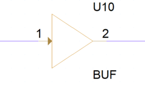
Buffers are commonly used for:
- Strengthening and amplifying digital signals
- Increasing the number of inputs that a signal can drive without degrading signal quality
Inverter
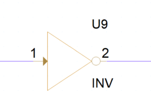
Inverters are commonly used for:
- Inverting an input signal
- Converting between different logic levels
What is Needed to Model a Buffer or Inverter?
Buffer and inverter models are frequently used for digital applications as both components are essential building blocks in digital circuitry to ensure reliable signal transmission. To realistically simulate digital circuit functionality and create a buffer or inverter SPICE model for simulation, there are three items that must be defined:
Timing Characteristics
Timing is critical to digital design operation and performance. Consider the delay caused by the buffer or inverter.
DC Electrical Characteristics
The DC electrical characteristics define the operating conditions for the buffer or inverter. This includes:
- The maximum output voltages during high-level and low-level operation for the buffer or inverter
- The voltage levels or thresholds that control the switch from high-level operation to low-level operation
- Hysteresis is often defined for these devices to provide a cushion, ensuring accurate switching between low-level and high-level states even with noisy input signals. It is typically provided by device manufacturers on the device datasheet as VH; however, if not provided it can be calculated by the following equation: VH = VT+ – VT-
Device Resistance
Input and output resistance of the device is critical to the operation and necessary to create an accurate model representation. If this parameter is not provided on the device datasheet, it can be calculated with Ohm’s law.
Input Resistance (Rin)
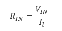
Use the maximum input voltage (VIN) and maximum leakage current (commonly IIN or Il) to calculate the input resistance.
Output Resistance (Rout)
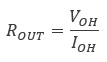
Use the maximum output voltage (VOH or VOL) and the maximum output current (IOH or IOL) to calculate the output resistance.
Once this information is obtained and calculated, these values must be incorporated into the SPICE simulation model which can be achieved by manually creating or editing a text file. Keep in mind if the buffer or inverter created does not produce the intended outcome and a decision is made to change components, values will need to be re-calculated and edited manually. This manual process to produce an accurate buffer or inductor model is time consuming and increases the likelihood of errors; however, the PSpice Modeling App provides a fast, easily configurable, and fully integrated method to create buffer or inverter models for simulation.
Creating a Buffer or Inverter SPICE Model in PSpice
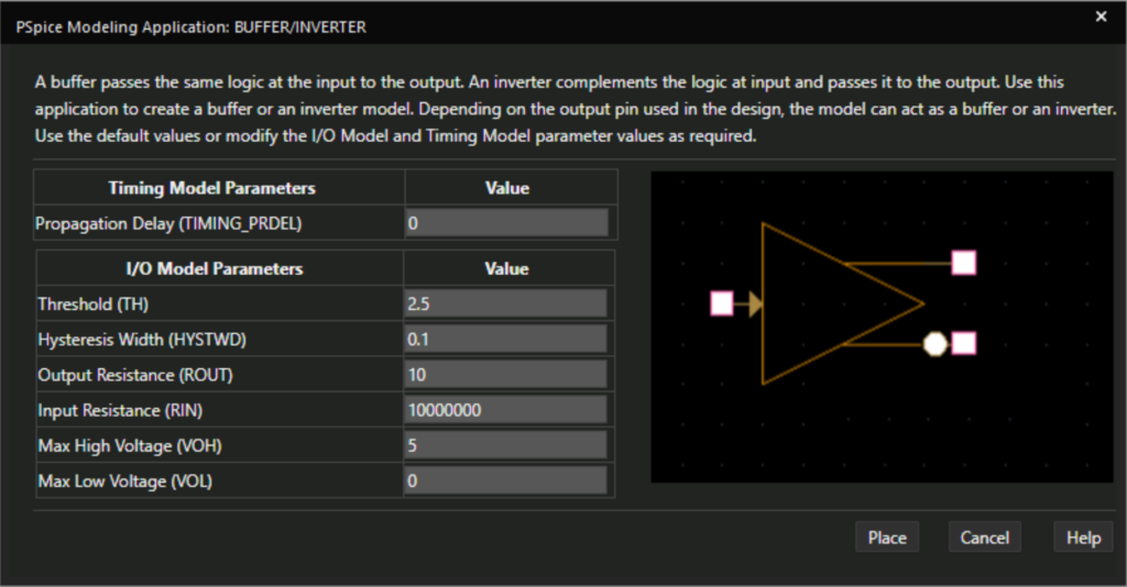
The buffer/inverter modeling application quickly creates buffer or inverter SPICE models with a wizard-based approach. To create buffer or inverter models, users can easily input the characteristics, defined by manufacturers, directly into predefined parameters:
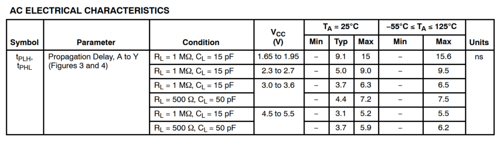
Propagation Delay
Define the time delay between the input and output pins of the device. This is typically defined as tPLH or tPHL on device datasheets.
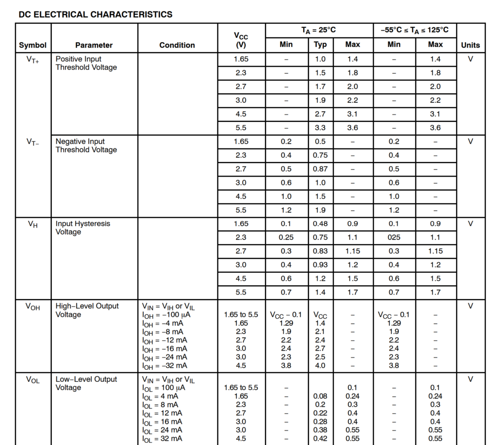
Threshold (TH)
Define the voltage level that indicates a switch between high-level and low-level operation.
Hysteresis Width
Hysteresis is the difference between the positive input threshold voltage and the negative input threshold voltage. It is typically provided on the device datasheet as VH.
Max High Voltage
Define the maximum voltage output during high-level operation. This is typically defined on device datasheets as VOH.
Max Low Voltage
Define the maximum voltage output during low-level operation. This is typically defined on device datasheets as VOL.
Output Resistance (Rout)
Specify the resistance of the output pin.
Input Resistance (Rin)
Specify the resistance of the input pin.
Using the inputted information above, the PSpice Modeling App generates a schematic symbol and automatically associates the newly created buffer or inverter SPICE model without leaving the OrCAD Capture environment. The PSpice Modeling App also automatically manages the simulation profile configuration, eliminating any library set up for simulation.
Download the free trial of OrCAD to try it yourself.
Get the step-by-step instructions for creating a Buffer or Inverter SPICE Model here.