At the beginning of every new year, we tend to be very optimistic for the future. In order to move forward into 2017, we thought it was a good time to reflect back on the evolution of PCB design and how these changes are expected to shape the future of the industry.
In order to meet the increasing needs of the electronics market, companies have expanded and PCB design engineers are in high demand. To get a better perspective on these changes, we interviewed some of our in-house engineers who entered the industry at different points in time: Applications Engineers’ Rocco Calvello and Matthew Harms, and Sr. Technical Support Specialist, Bill Stuhler.
Q1. How long have you worked in the PCB industry?
Rocco Calvello: 30 Years
Matthew Harms: 15 years
Bill Stuhler: I started by accident when I was 18 years old, so 52 years ago
Q2. What was your first PCB experience?
RC: Building my own PCB (radio project) in my electronics class.
MH: As an engineer, the PCB just ‘magically’ appears. My first experience was designing a small board and later seeing the physical board that it had become. It was interesting to see what all happens after the schematic gets completed
BS: My first board design was for a board used in an instrument that could look at a color sample and tell you exactly what mixtures of paint was needed to duplicate it. It was agreed upon by my supervisor and the engineer in charge of the project that as it was my first design that it did not matter how long it took as long as I completed it. About half way through I was ready to give up, I was encouraged to continue on. If took me 5 weeks from the start to the last piece of crepe tape was on the matt film used to generate the artwork.
Q3. In your opinion what has been the most revolutionary change in the PCB industry in your lifetime?
RC: Package density and new package technology as well as the ability to manufacture very small geometries.
MH: Integration of different disciplines. Engineers now want instant visibility into corporate purchasing systems and back and forth communication with the mechanical CAD team.
BS: When I started, board designs were designed on gridded paper with multiple colored pencils on a 2 times size scale and then taped on matt film that would be sent out to be photographed at the true 1-time size scale. The advent of the computer and the computer-aided software for this purpose was probably the first big improvement in the creation of board design.
Follow-up question: Why is that a revolutionary change and how does that help further the industry?
RC: Advances in chip technology has provided much more functionality in the chip die, which translates to smaller device packages at the PCB level. One example would be hand-held devices such as cell phones employ many of these advances. They have gotten so much smaller over the years with much more capabilities and with less power consumption.
MH: This is revolutionary because it gives engineers access to information that they didn’t have before (like costing and component heights) to reduce spending where possible and prevent physical violations. This means that companies can continue to get their products to market cheaper (by buying less expensive components) and faster (by eliminating re-spins due to physical conflicts).
BS: The computer-aided software for the design of a board design has reduced the time frame for a board design from weeks to a matter of a few days.
Q4. From your experience in the industry, how has PCB design changed and/or remained the same?
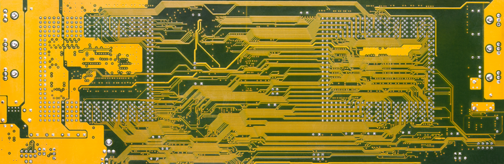
RC: PCB design construction remains the same, but the number of layers has increased, trace width and spacing have become smaller.
MH: Changed – everything is done on a computer now.
BS: The speed and complexity of designs now are far greater than when I started.
Follow-up question: What challenges arise because of that? And How are they affected by this change?
RC: Manufacturing is clearly impacted by these changes, the manufacturer needs to have the latest most accurate equipment and processes to reliably produce products with good yields.
MH: The challenge is that engineers and layout designers need to be proficient in the CAD tool that they’re using to most quickly communicate their design intent to the software. CAD tools by the same measure need to be easy to use but also functional enough to handle to most challenging designs so the engineers are not held back. The effect is boards that are vastly more complex than their predecessors while not requiring a significant uptick in staff to create them.
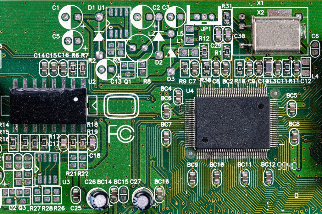
BS: Back when I was designing boards a major design might have a couple of hundred parts making up the design. Now it is not unusual to have a design with thousands of parts in them.
Q5. How do you expect the industry to change or evolve in the next 10 years?
RC: We will continue to make advances in manufacturing smaller devices, with lower power consumption, and higher functionality.
MH: Smaller, Faster, Cheaper. More integration and fewer ECAD vendors
BS: As has happened over the last 10 to 15 years the number of board design software companies is going to continue to decrease. Over the last 10 to 15 years the number of companies providing this software have decreased through mergers and takeovers.
According to a recent market report by Technavio, the global printed circuit board market is expected to grow at a CAGR rate of 3% by 2020. This growth is predicted based on the increase in demand for IoT devices, wearables, and other advanced technologies. The anticipated highest revenue contributor for the PCB market in this timeframe is the networking and communication segment, expected to account for a revenue share of around 30% by 2020.
With these thoughts in mind, the future of the PCB Industry has a very positive outlook. Going forward engineers and technical specialists alike have a lot to look forward to as the industry continues to evolve with an increased focus on technological advances. For the latest updates and industry trends sign up for our newsletter below.