Designing high-power PCBs presents numerous challenges, including managing heat, ensuring signal integrity, and maintaining safety. High currents generate significant heat, necessitating efficient thermal management strategies like wider traces, thermal vias, and heat sinks to prevent overheating and ensure reliable operation. Signal integrity can be compromised due to high currents causing electromagnetic interference (EMI), requiring careful layout, proper grounding, and shielding techniques. Maintaining adequate spacing between high voltage traces is also crucial to prevent arcing and ensure safety, while adhering to relevant standards and regulations. Balancing these factors while achieving a compact, efficient design requires meticulous planning and expertise. The table below examines the best high-power PCB design guidelines for engineers to follow to achieve these goals.
Best High-Power PCB Design Guidelines | ||
Category | Guidelines | Benefit |
| Trace Design | ✔ Use wider traces to handle higher currents | + Prevents overheating and ensures safe current handling |
Thermal Management | ✔ Use thermal vias to transfer heat from top layer to inner layers | + Improves heat dissipation and prevents component overheating |
Component Placement | ✔ Place high-power components to minimize thermal interference | + Prevents heat build-up and maintains uniform temperature |
Power Plane Design | ✔ Use multiple layers for power and ground planes | + Ensures stable power delivery and reduces voltage fluctuations |
Via Design | ✔ Use multiple vias to reduce resistance and increase capacity | + Ensures reliable current conduction/reduces thermal stress |
Grounding | ✔ Implement a solid ground plane to reduce noise/improve stability | + Provides a low-impedance path for return currents, reducing noise |
Current Carrying Capacity | ✔ Ensure traces can handle the required current | + Prevents trace damage and ensures safe operation |
Electromagnetic Interference (EMI) | ✔ Shield high-power traces and components to reduce EMI. | + Prevents interference with other circuits and devices |
Thermal Relief Pads | ✔ Use thermal relief pads to aid in soldering high-power components. | + Ensures reliable solder joints and reduces thermal stress. |
Safety | ✔ Ensure adequate spacing between high voltage traces. | + Prevents electrical shorts and ensures user safety. |
These guidelines help ensure the reliability and performance of high-power PCB designs by addressing key factors such as thermal management, component placement, trace design, and safety considerations.
High-Power PCB Design Guidelines and PCB Software
The right PCB design software is crucial for high-power PCB design, because it ensures precision and efficiency in managing complex electrical requirements. High-power PCBs require accurate trace width calculations, optimal component placement, and effective thermal management. Specialized software offers advanced tools for these tasks, such as automated trace width calculations based on current capacity and real-time simulations for thermal analysis. This precision helps prevent overheating and electrical failures.
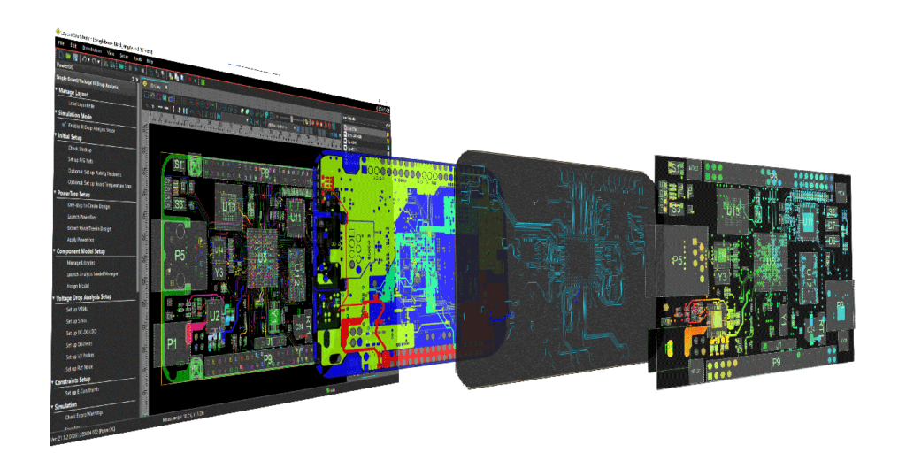
The right simulation software aids in maintaining the integrity and reliability of the PCB design throughout the development process. High-power PCB designs often require multiple iterations and detailed testing to meet performance and safety standards. Advanced software solutions provide features like automatically verifying that the design adheres to industry standards and guidelines. Other features include version control and collaboration tools that allow multiple engineers to work on the same project simultaneously, ensuring consistency and reducing the risk of errors.
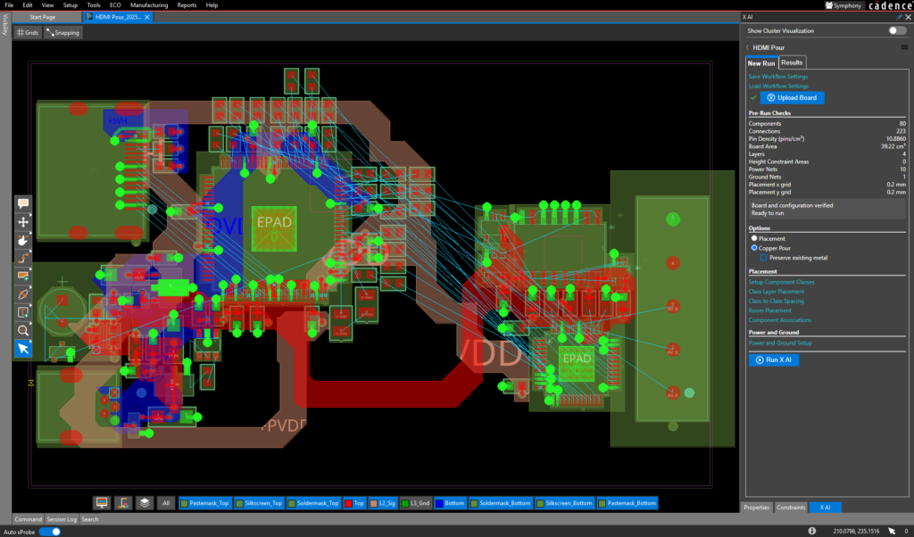
With software features like automated routing, component library management, and integration with simulation tools, engineers can streamline their workflow and focus on optimizing the design. These tools also facilitate easy modifications and updates, which are common in high-power PCB projects due to evolving requirements and specifications. By leveraging the right software, companies can accelerate their development cycles, reduce costs, and ensure that their high-power PCB designs are robust, reliable, and compliant with industry standards.
EMA Design Automation is a leading provider of the resources that engineers rely on to accelerate innovation. We provide solutions that include PCB design and analysis packages, custom integration software, engineering expertise, and a comprehensive academy of learning and training materials, which enable you to create more efficiently. For more information on PCB design flow optimization and how we can help you or your team innovate faster, contact us.
