Circuit noise is unwanted electrical signals that interfere with electronic circuits. This noise can originate from various sources, including electromagnetic interference (EMI), radio frequency (RF) interference, power supply fluctuations, or internal circuit components. Without proper circuit noise reduction techniques, noise can cause data corruption, signal distortion, component malfunction, or even complete system failure.
Circuit Noise Reduction Techniques Identified
Employing circuit noise reduction techniques is critical to ensure the reliability, accuracy, and stability of electronic devices, especially in high-speed communication systems, precision measurement tools, and safety-critical applications like medical devices or automotive electronics. Below are common circuit noise reduction techniques and their applications.
Circuit Noise Reduction Techniques | ||
Techniques | Description | Application |
| Grounding and Shielding | Proper grounding and conductive shields to minimize noise from external sources. | High-frequency circuits, communication systems, and audio equipment to protect from EMI. |
Decoupling Capacitors | Capacitors placed close to power pins to filter out noise and provide a smooth voltage supply. | Digital and analog circuits to reduce power supply noise, especially for ICs requiring stable voltage. |
Twisted Pair Cables | Two wires twisted together to cancel out EMI. | Communication cables, Ethernet, and other signal-carrying systems to minimize interference. |
Differential Signaling | Two complementary signals that cancel out common-mode noise. | Applied in data transmission standards like USB, HDMI, and Ethernet to reduce high-speed signal noise. |
Ferrite Beads | Small inductive components that block high-frequency noise from power or signal lines. | Power supplies, USB cables, and signal paths to suppress RF interference. |
Low-Pass Filters | Filters that enable low frequencies to pass while blocking high-frequency noise. | Audio systems, power supplies, and communication systems to reduce high-frequency interference. |
Spread Spectrum Clocking | Spreading out clock signal frequency spectrum to reduce noise energy at any given frequency. | Systems that need to minimize EMI, such as RF and communication systems. |
Capacitive Coupling | Capacitors that block DC components and pass AC signals, isolating noise sources. | Signal lines and amplifier circuits to prevent unwanted DC signals from introducing noise. |
Signal Termination | Matching the impedance of a transmission line to prevent signal reflections that can cause noise. | High-speed signal interfaces to reduce reflections and associated noise. |
Power Supply Noise Isolation | Isolation between noisy and quiet power supplies using separate regulators or transformers. | Mixed-signal circuits, analog-to-digital converters, and sensitive analog circuitry. |
How To Conduct Circuit Noise Analysis
Conducting circuit noise analysis involves identifying, measuring, and mitigating circuit noise sources to ensure proper functionality. Here’s a step-by-step process:
Enhanced Design Automation and Efficiency
1) Identify Potential Noise Sources
✔ Internal Sources: Look for switching components (like transistors, relays, or power regulators), high-frequency clocks, and power supply ripples that can generate noise within the circuit.
✔ External Sources: Consider noise from external EMI, RF interference, or even environmental factors like temperature changes.
2) Analyze Signal Paths
✔ PCB Layout Inspection: Review the circuit layout to identify long traces, signal crossovers, and improper grounding, which can contribute to noise coupling.
✔ Impedance Mismatches: Mismatches in transmission lines can cause signal reflections that increase noise.
✔ Ground Loops: Ensure there are no unintended ground loops that could pick up noise or create voltage differentials.
3) Measure Noise
✔ Oscilloscope: Use an oscilloscope to inspect the signals on critical parts of the circuit visually. High-frequency noise or spikes can be detected in the time domain.
✔ Spectrum Analyzer: Use a spectrum analyzer to identify noise across a frequency range. This helps pinpoint EMI or RF interference that might not be visible in time-domain measurements.
✔ Signal Integrity Tools: Employ SI tools to model and simulate noise effects in different circuit parts.
4) Quantify the Impact
✔ Noise Margin: Calculate the noise margin for digital circuits (difference between actual voltage and threshold levels) to see if the system can tolerate noise without signal degradation.
✔ Power Supply Noise: Measure the ripple and fluctuations in the power supply, which can directly impact sensitive components.
✔ Crosstalk: Assess how signals on one trace or wire can affect adjacent signals, especially in densely packed PCB layouts.
5) Apply Mitigation Techniques
Apply appropriate noise reduction techniques based on the findings (see Table above).
6) Validate with Simulation
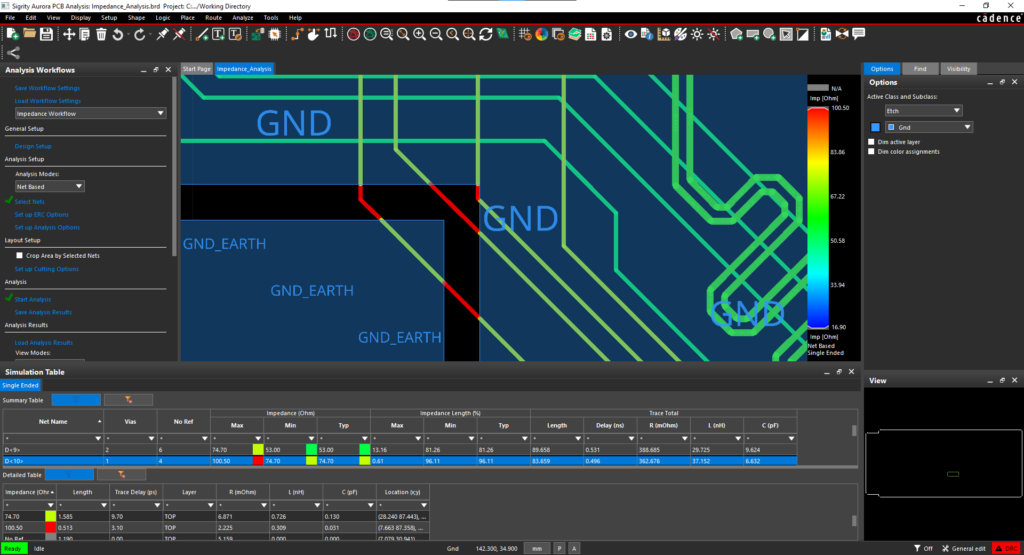
Use simulation tools like Sigrity X to test noise mitigation techniques before physical implementation. Sigrity offers features like:
✔ In-design Analysis: Provides analysis directly in the PCB canvas for crosstalk, reflection, IR drop, return path, and power inductance
✔ SPICE-based Simulator: Provides a SPICE-based simulator and embedded hybrid field solvers for extracting 2D and 3D structures
✔ Power-aware IBIS Models: Supports power-aware IBIS models, as well as transistor-level models
✔ Reflection analysis: Simulates designs to find issues like reflection and ringing and compares the impact of each on signal reflections
✔ Return Path Analysis: Identifies signals where current returns inefficiently
By following these six steps, engineers can identify noise issues and reduce their impact on overall circuit performance.
EMA Design Automation is a leading provider of the resources that engineers rely on to accelerate innovation. We provide solutions that include PCB design and analysis packages, custom integration software, engineering expertise, and a comprehensive academy of learning and training materials, which enable you to create more efficiently. For more information on PCB design flow optimization and how we can help you or your team innovate faster, contact us.


