Adventures in Backdrilling
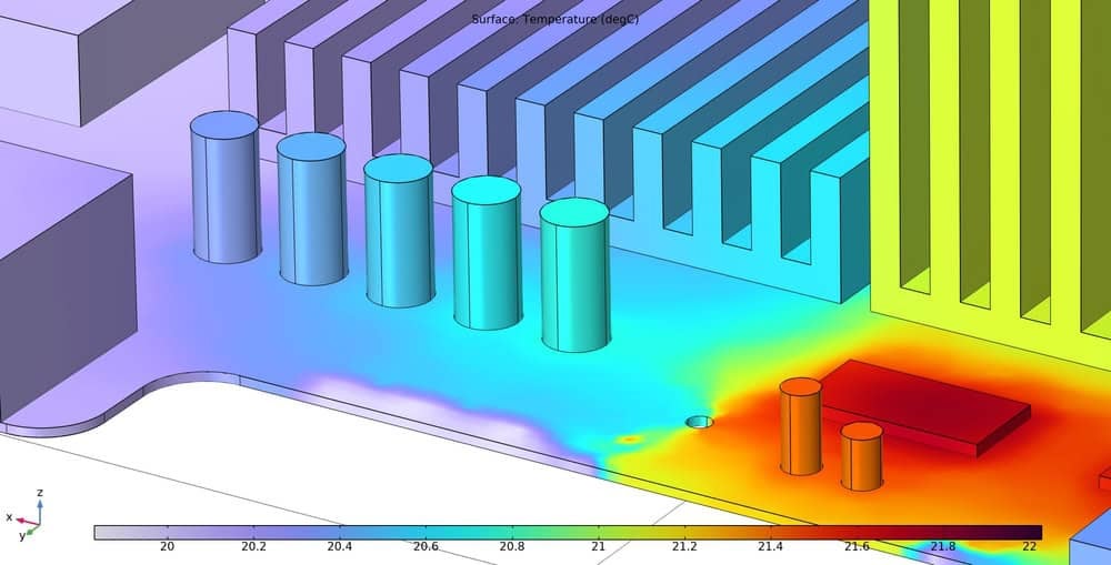
For the past 15 years or so, routing high-speed interfaces handling 5Gbps or higher have become more common in many electrical designs. Transitioning high-frequency signals between layers can greatly affect signal integrity when a portion of plated through-hole (PTH) is left unused, forming an electrical stub. In general, these stubs are a source of impedance discontinuities and signal reflections, which become more critical as data rates increase.

What options do I have to eliminate the electrical stub?
• Use a board fabrication process called backdrilling, sometimes referred to as controlled depth counter-boring.
• Carefully plan/restrict the high-speed interface routing to certain layers to minimize the stub effects.
• Use Blind, Buried and Micro vias technologies for routing high-speed signals which has its share of limitations, concerns and added fabrication costs while not addressing press fit connector pins which commonly require backdrilling to eliminate the electrical stub.
In the early years, the fabrication vendor would identify backdrill opportunities based on critical net list and make all the appropriate adjustments.
Introducing a backdrill process to a design can sometimes be a nightmare to manage and requires working very closely with your fabrication vendor. The fabrication vendor will remove as much stub as possible on the identified high-speed signals, adjusting features at each backdrill location and verifying copper clearances due to the increased backdrill size to maintain design integrity.
To ease a transition to a more streamlined process, a stable foundation was developed in Allegro 15.7 to reduce the post processing of data at the fabrication vendor.
As a previous customer, I was part of the Allegro® PCB Designer 15.7 Beta Test Team in late 2005. I was very excited to see/test the new Backdrill solution inside of Allegro. The functionality pushed Allegro to a higher level by allowing designers to identify nets that require Backdrilling and apply several component and pin properties to influence the design analysis to identify backdrill locations. Locations were identified in the Backdrill report, marked by special backdrill figures/legends for documentation and accompanied with manufacturing NCDrill files of backdrill locations for each specific depth. Even with these enhancement there was still a number of manual steps to ensure the design integrity is maintained (supporting multiple padstacks for backdrill locations, manual backdrill keepouts and backdrill size adjustments at the fabricator)
As time went on, it was clear that further enhancements would improve the process by providing functionality to not only analyze design but also adjust features at the backdrill locations along with generation of a complete manufacturing data package to streamline the fabrication process.
Cadence worked with fabricators and customers to fine tune the existing solution to not only remove most of the post-processing steps by the fabricator but also enhance several areas of the tool in support of the backdrill process. As a member of Product Engineering, I was able to influence the functionality based on my own past customer experiences as well as gathering feedback from our customers.
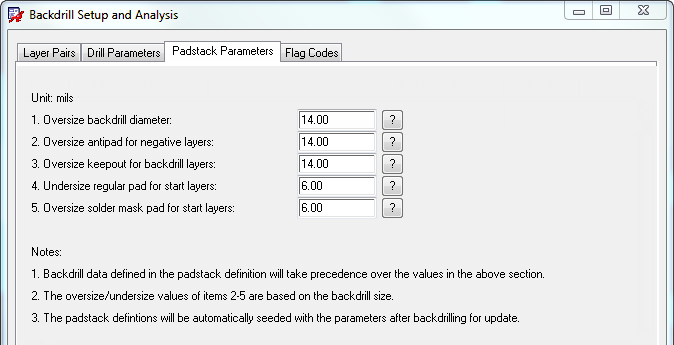
- Padstack supports the definition of backdrill data at the library.
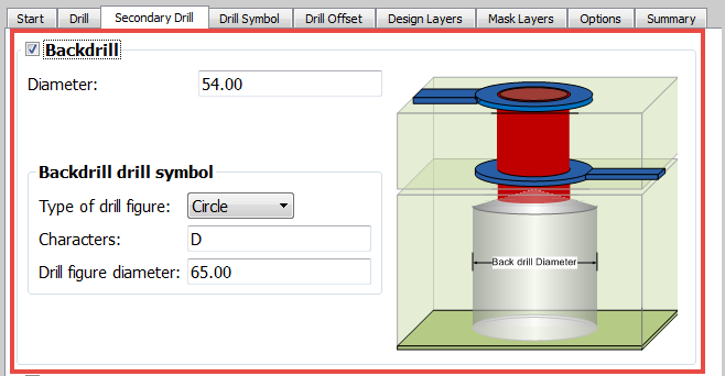
- Backdrill size with unique drill figures
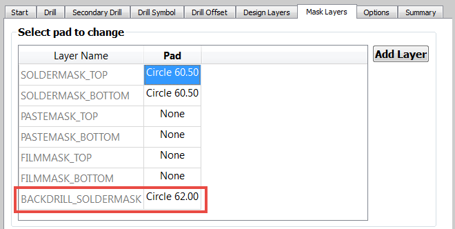
- Backdrill entry pad and Solder mask enhancements
- Layer keepouts / clearance additions

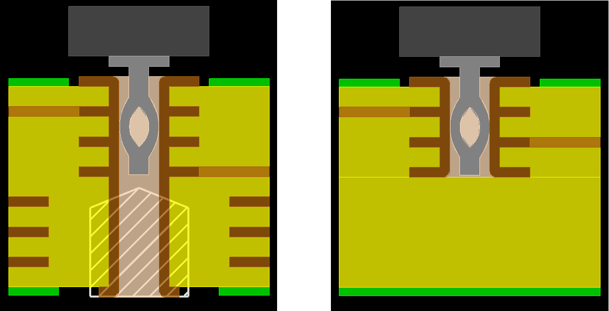
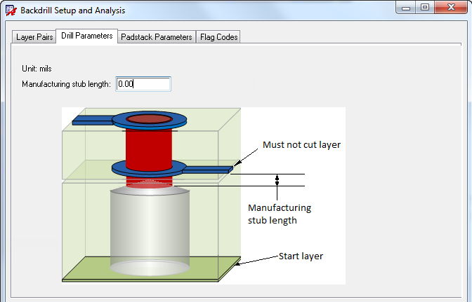
Typical Backdrill Location
- Manufacturing stub length – remaining stub length after backdrill (advanced configuration)
- Remaining manufacturing stub length measured down from the Must Not Cut Layer, which acts as a target backdrill depth into the dielectric
- Parameter based design level padstack updates built into Backdrill analysis.
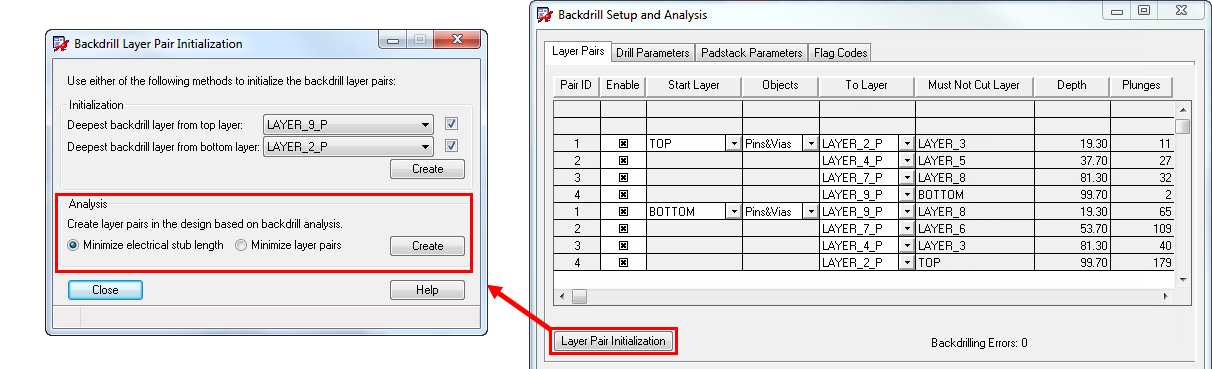
- Improved model to quickly define / review backdrill layer pairs based on design analysis
- Initialization: Deepest backdrill layer from top and bottom layers
- Analysis: Minimized electrical stub length or minimize layer pair
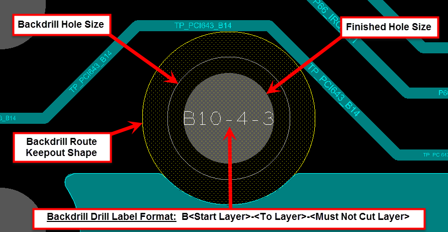
- Backdrill diameter displayed with special drill labels to identify backdrill side/depth.
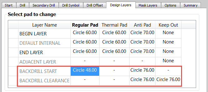
- Route keepouts automatically generated based on clearance defined in padstack
- No more creating special padstacks or keepouts at backdrill sites.
- Show Element reports all backdrill data attached to pins/vias at backdrill locations
- Actual backdrill size is now reported in drill legends and manufacturing NCDrill files based on backdrill data defined in padstack
- No longer necessary for fabrication vendor to adjust sizes based on plated through-hole
- Backdrill Legends now reports the Must Not Cut Layer, depth and manufacturing stub information
- Fabrication drawing cross-section detail now reports backdrill spans
- Full Test Point awareness during backdrilling process
- No drilling away a test point or adding test points at backdrill sites.
This new enhanced backdrill solution takes all of the guess work and stress associated with introducing Backdrilling in a design. No more increased Non-Recurring Engineering (NRE) charges at the fabricator, no more escalating costs associated with introducing different via and build-up technologies. Lastly a more complete manufacturing data package with backdrill data information contained in IPC-D-356 and IPC-2581 along with full documentation communicating backdrill intent to the fabricator.
Watch the related Backdrill Demo Reel video